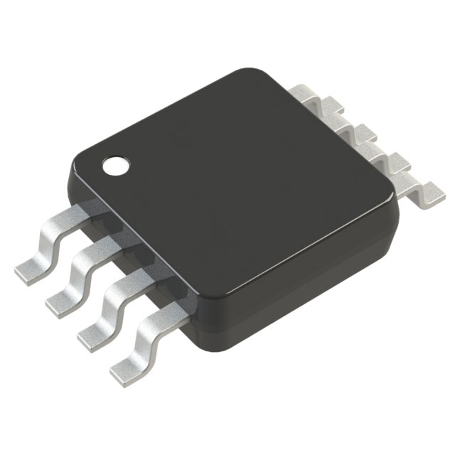
AD7887ARMZ
Active2-CHANNEL SINGLE ADC SAR 125KSPS 12-BIT SERIAL 8-PIN MSOP TUBE
Deep-Dive with AI
Search across all available documentation for this part.

AD7887ARMZ
Active2-CHANNEL SINGLE ADC SAR 125KSPS 12-BIT SERIAL 8-PIN MSOP TUBE
Deep-Dive with AI
Technical Specifications
Parameters and characteristics for this part
| Specification | AD7887ARMZ |
|---|---|
| Architecture | SAR |
| Configuration | MUX-S/H-ADC |
| Data Interface | DSP, SPI |
| Input Type | Single Ended |
| Mounting Type | Surface Mount |
| Number of A/D Converters | 1 |
| Number of Bits | 12 bits |
| Number of Inputs | 1, 2 |
| Operating Temperature [Max] | 125 °C |
| Operating Temperature [Min] | -40 °C |
| Package / Case | 8-MSOP, 8-TSSOP |
| Package / Case | 3 mm |
| Package / Case [custom] | 0.118 in |
| Ratio - S/H:ADC | 1:1 |
| Reference Type | External, Internal |
| Supplier Device Package | 8-MSOP |
| Voltage - Supply, Analog [Max] | 5.25 V |
| Voltage - Supply, Analog [Min] | 2.7 V |
| Voltage - Supply, Digital [Max] | 5.25 V |
| Voltage - Supply, Digital [Min] | 2.7 V |
Pricing
Prices provided here are for design reference only. For realtime values and availability, please visit the distributors directly
| Distributor | Package | Quantity | $ | |
|---|---|---|---|---|
| Digikey | Tube | 1 | $ 16.24 | |
| 10 | $ 11.65 | |||
| 25 | $ 10.47 | |||
| 100 | $ 9.15 | |||
| 250 | $ 8.51 | |||
| 500 | $ 8.12 | |||
| 1000 | $ 8.04 | |||
Description
General part information
AD7887 Series
The AD7887 is a high speed, low power, 12-bit analog-to-digital converter (ADC) that operates from a single 2.7 V to 5.25 V power supply. The AD7887 is capable of 125 kSPS throughput rate. The input track-and-hold acquires a signal in 500 ns and features a single-ended sampling scheme. The output coding for the AD7887 is straight binary, and the part is capable of converting full power signals of up to 2.5 MHz.The AD7887 can be configured for either dual- or single-channel operation via the on-chip control register. There is a default single-channel mode that allows the AD7887 to be operated as a read-only ADC. In single-channel operation, there is one analog input (AIN0) and the AIN1/VREFpin assumes its VREFfunction. This VREFpin allows the user access to the part’s internal 2.5 V reference, or the VREFpin can be overdriven by an external reference to provide the reference voltage for the part. This external reference voltage has a range of 2.5 V to VDD. The analog input range on AIN0 is 0 to VREF.In dual-channel operation, the AIN1/VREFpin assumes its AIN1 function, providing a second analog input channel. In this case, the reference voltage for the part is provided via the VDDpin. As a result, the input voltage range on both the AIN0 and AIN1 inputs is 0 to VDD.CMOS construction ensures low power dissipation of typically 2 mW for normal operation and 3 μW in power-down mode. The part is available in an 8-lead, 0.15-inch-wide narrow body SOIC and an 8-lead MSOP package.Product HighlightsSmallest 12-bit dual-/single-channel ADC; 8-lead MSOP package.Lowest power 12-bit dual-/single-channel ADC.Flexible power management options, including automatic power-down after conversion.Read-only ADC capability.Analog input range from 0 V to VREF.Versatile serial input/output port (SPI/QSPI/MICROWIRE/ DSP compatible).ApplicationsBattery-powered systems (personal digital assistants, medical instruments, mobile communications)Instrumentation and control systemsHigh speed modems
Documents
Technical documentation and resources


