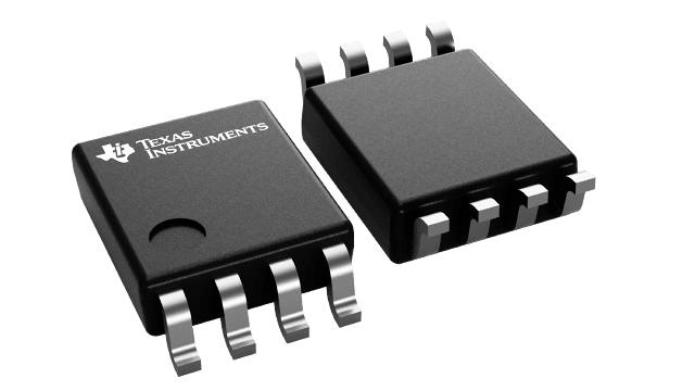
SN74LVC2G79DCURG4
UnknownDUAL POSITIVE-EDGE-TRIGGERED D-TYPE FLIP-FLOP
Deep-Dive with AI
Search across all available documentation for this part.

SN74LVC2G79DCURG4
UnknownDUAL POSITIVE-EDGE-TRIGGERED D-TYPE FLIP-FLOP
Deep-Dive with AI
Technical Specifications
Parameters and characteristics for this part
| Specification | SN74LVC2G79DCURG4 |
|---|---|
| Clock Frequency | 160 MHz |
| Current - Output High, Low [x] | 32 mA |
| Current - Output High, Low [y] | 32 mA |
| Current - Quiescent (Iq) | 5 µA |
| Function | Standard |
| Input Capacitance | 3.5 pF |
| Max Propagation Delay @ V, Max CL | 4.5 ns |
| Mounting Type | Surface Mount |
| Number of Bits per Element | 1 |
| Number of Elements | 2 |
| Operating Temperature [Max] | 125 °C |
| Operating Temperature [Min] | -40 °C |
| Output Type | Non-Inverted |
| Package / Case | 8-VFSOP |
| Package / Case [y] | 2.3 mm |
| Package / Case [y] | 0.091 in |
| Trigger Type | Positive Edge |
| Type | D-Type |
| Voltage - Supply [Max] | 5.5 V |
| Voltage - Supply [Min] | 1.65 V |
Pricing
Prices provided here are for design reference only. For realtime values and availability, please visit the distributors directly
| Distributor | Package | Quantity | $ | |
|---|---|---|---|---|
| Digikey | Tape & Reel (TR) | 3000 | $ 0.30 | |
| 6000 | $ 0.28 | |||
| 15000 | $ 0.27 | |||
| 30000 | $ 0.26 | |||
| Texas Instruments | LARGE T&R | 1 | $ 0.51 | |
| 100 | $ 0.39 | |||
| 250 | $ 0.29 | |||
| 1000 | $ 0.20 | |||
Description
General part information
SN74LVC2G79 Series
This dual positive-edge-triggered D-type flip-flop is designed for 1.65-V to 5.5-V VCCoperation.
When data at the data (D) input meets the setup time requirement, the data is transferred to the Q output on the positive-going edge of the clock pulse. Clock triggering occurs at a voltage level and is not directly related to the rise time of the clock pulse. Following the hold-time interval, data at the D input can be changed without affecting the levels at the outputs.
NanoFree™ package technology is a major breakthrough in IC packaging concepts, using the die as the package.
Documents
Technical documentation and resources


