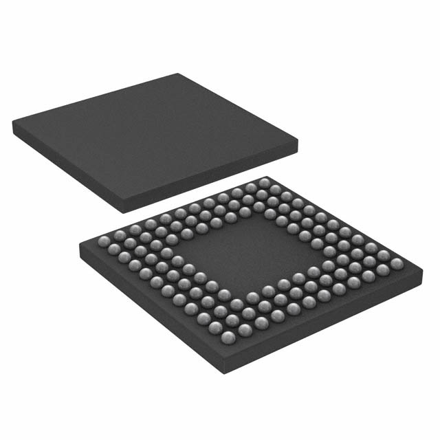
AD5378ABCZ
Active32-CHANNEL 14-BIT SERIAL/PARALLEL BIPOLAR D/A CONVERTER
Deep-Dive with AI
Search across all available documentation for this part.

AD5378ABCZ
Active32-CHANNEL 14-BIT SERIAL/PARALLEL BIPOLAR D/A CONVERTER
Technical Specifications
Parameters and characteristics for this part
| Specification | AD5378ABCZ |
|---|---|
| Architecture | String DAC |
| Data Interface | DSP, SPI |
| Differential Output | False |
| INL/DNL (LSB) | 3 LSB |
| INL/DNL (LSB) [Max] | 1.5 LSB |
| INL/DNL (LSB) [Min] | -1 LSB |
| Mounting Type | Surface Mount |
| Number of Bits | 14 |
| Number of D/A Converters | 32 |
| Operating Temperature [Max] | 85 °C |
| Operating Temperature [Min] | -40 °C |
| Output Type | Voltage - Buffered |
| Package / Case | 108-BGA, CSPBGA |
| Reference Type | External |
| Settling Time | 30 µs |
| Voltage - Supply, Analog [Max] | 16.5 V |
| Voltage - Supply, Analog [Min] | -3 V, 8.5 V |
| Voltage - Supply, Digital [Max] | 5.5 V |
| Voltage - Supply, Digital [Min] | 2.7 V |
Pricing
Prices provided here are for design reference only. For realtime values and availability, please visit the distributors directly
Description
General part information
AD5378 Series
The AD5378 contains 32 14-bit DACs in one CSPBGA package. The AD5378 provides a bipolar output range determined by the voltages applied to the VREF(+) and VREF(−) inputs. The maximum output voltage span is 17.5 V, corresponding to a bipolar output range of −8.75 V to +8.75 V, and is achieved with reference voltages of VREF(−) = −3.5 V and VREF(+) = +5 V.The AD5378 guarantees operation over a wide VSS/VDDsupply range from ±11.4 V to ±16.5 V. The output amplifier headroom requirement is 2.5 V operating with a load current of 1.5 mA, and 2 V operating with a load current of 0.5 mA.The AD5378 contains a double-buffered parallel interface in which 14 data bits are loaded into one of the input registers under the control of theWR,CS, and DAC channel address pins, A0 to A7. It also has a 3-wire serial interface, which is compatible with SPI®, QSPI™, MICROWIRE™, and DSP interface standards and can handle clock speeds of up to 50 MHz.The DAC outputs are updated when the DAC registers receive new data. All the outputs can be updated simultaneously by taking theLDACinput low. Each channel has a programmable gain and an offset adjust register.Each DAC output is gained and buffered on-chip with respect to an external REFGND input. The DAC outputs can also be switched to REFGND via theCLRpin. Table 1 and Table 2 show the product portfolio for high channel count bipolar and unipolar voltage output DACs.APPLICATIONSLevel setting in automatic test equipment (ATE)Variable optical attenuators (VOAs)Optical switchesIndustrial control systems


