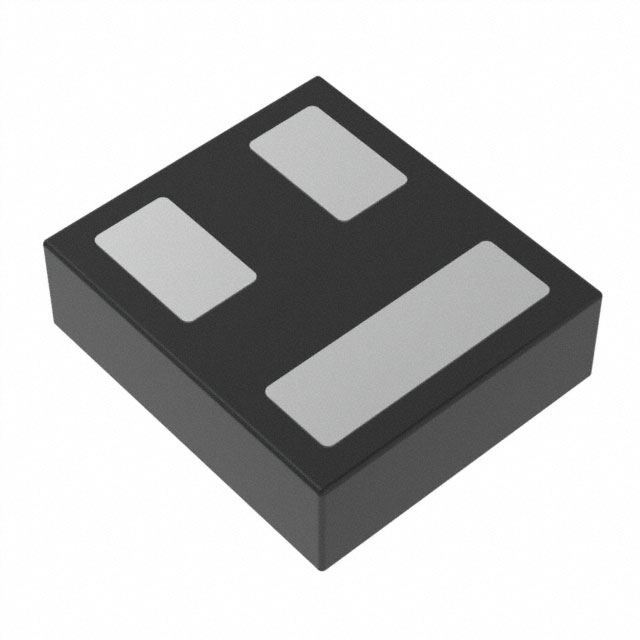
CSD25501F3T
Active-20-V, P CHANNEL NEXFET™ POWER MOSFET, SINGLE LGA 0.6 MM X 0.7 MM, 76 MOHM, GATE ESD PROTECTION
Deep-Dive with AI
Search across all available documentation for this part.

CSD25501F3T
Active-20-V, P CHANNEL NEXFET™ POWER MOSFET, SINGLE LGA 0.6 MM X 0.7 MM, 76 MOHM, GATE ESD PROTECTION
Deep-Dive with AI
Technical Specifications
Parameters and characteristics for this part
| Specification | CSD25501F3T |
|---|---|
| Current - Continuous Drain (Id) @ 25°C | 3.6 A |
| Drain to Source Voltage (Vdss) | 20 V |
| Drive Voltage (Max Rds On, Min Rds On) | 4.5 V, 1.8 V |
| FET Type | P-Channel |
| Gate Charge (Qg) (Max) @ Vgs [Max] | 1.33 nC |
| Input Capacitance (Ciss) (Max) @ Vds | 385 pF |
| Mounting Type | Surface Mount |
| Operating Temperature [Max] | 150 °C |
| Operating Temperature [Min] | -55 °C |
| Package / Case | 3-XFLGA |
| Power Dissipation (Max) [Max] | 500 mW |
| Rds On (Max) @ Id, Vgs | 76 mOhm |
| Supplier Device Package | 3-LGA |
| Supplier Device Package [x] | 0.73 |
| Supplier Device Package [y] | 0.64 |
| Technology | MOSFET (Metal Oxide) |
| Vgs (Max) [Max] | -20 V |
| Vgs(th) (Max) @ Id | 1.05 V |
Pricing
Prices provided here are for design reference only. For realtime values and availability, please visit the distributors directly
| Distributor | Package | Quantity | $ | |
|---|---|---|---|---|
| Digikey | Cut Tape (CT) | 1 | $ 0.86 | |
| 10 | $ 0.70 | |||
| 100 | $ 0.55 | |||
| Digi-Reel® | 1 | $ 0.86 | ||
| 10 | $ 0.70 | |||
| 100 | $ 0.55 | |||
| Tape & Reel (TR) | 250 | $ 0.54 | ||
| 500 | $ 0.46 | |||
| 1250 | $ 0.38 | |||
| 2500 | $ 0.35 | |||
| 6250 | $ 0.34 | |||
| 12500 | $ 0.32 | |||
| 25000 | $ 0.32 | |||
| Texas Instruments | SMALL T&R | 1 | $ 0.79 | |
| 100 | $ 0.51 | |||
| 250 | $ 0.39 | |||
| 1000 | $ 0.26 | |||
Description
General part information
CSD25501F3 Series
This –20V, 64mΩ, P-Channel FemtoFET™ MOSFET is designed and optimized to minimize the footprint in many handheld and mobile applications. This technology is capable of replacing standard small signal MOSFETs while providing a substantial reduction in footprint size. The integrated 10kΩ clamp resistor (RC) allows the gate voltage (VGS) to be operated above the maximum internal gate oxide value of –6V, depending on duty cycle. The gate leakage (IGSS) through the diode increases as VGS is increased above –6V.
This –20V, 64mΩ, P-Channel FemtoFET™ MOSFET is designed and optimized to minimize the footprint in many handheld and mobile applications. This technology is capable of replacing standard small signal MOSFETs while providing a substantial reduction in footprint size. The integrated 10kΩ clamp resistor (RC) allows the gate voltage (VGS) to be operated above the maximum internal gate oxide value of –6V, depending on duty cycle. The gate leakage (IGSS) through the diode increases as VGS is increased above –6V.
Documents
Technical documentation and resources


