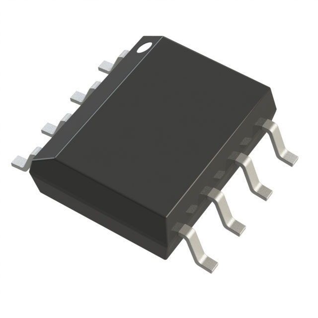
AD8557ARZ
ActiveDIGITALLY PROGRAMMABLE SENSOR SIGNAL AMPLIFIER
Deep-Dive with AI
Search across all available documentation for this part.

AD8557ARZ
ActiveDIGITALLY PROGRAMMABLE SENSOR SIGNAL AMPLIFIER
Deep-Dive with AI
Technical Specifications
Parameters and characteristics for this part
| Specification | AD8557ARZ |
|---|---|
| Amplifier Type | Zero-Drift |
| Current - Input Bias | 18 nA |
| Current - Output / Channel | 55 mA |
| Current - Supply | 1.8 mA |
| Gain Bandwidth Product | 2 MHz |
| Mounting Type | Surface Mount |
| Number of Circuits | 1 |
| Operating Temperature [Max] | 125 °C |
| Operating Temperature [Min] | -40 °C |
| Package / Case | 8-SOIC |
| Package / Case [x] | 0.154 in |
| Package / Case [y] | 3.9 mm |
| Supplier Device Package | 8-SOIC |
| Voltage - Input Offset | 2 çV |
| Voltage - Supply Span (Max) [Max] | 5.5 V |
| Voltage - Supply Span (Min) [Min] | 2.7 V |
Pricing
Prices provided here are for design reference only. For realtime values and availability, please visit the distributors directly
| Distributor | Package | Quantity | $ | |
|---|---|---|---|---|
| Digikey | Tube | 1 | $ 9.21 | |
| 10 | $ 6.37 | |||
| 25 | $ 5.63 | |||
| 100 | $ 4.81 | |||
| 250 | $ 4.41 | |||
| 500 | $ 4.17 | |||
| 1000 | $ 3.97 | |||
| 2500 | $ 3.86 | |||
Description
General part information
AD8557 Series
The AD8557 is a zero drift, sensor signal amplifier with digitally programmable gain and output offset. Designed to easily and accurately convert variable pressure sensor and strain bridge outputs to a well-defined output voltage range, the AD8557 accurately amplifies many other differential or single-ended sensor outputs. The AD8557 uses the Analog Devices, Inc., proprietary low noise auto-zero and DigiTrim®technologies to create an accurate and flexible signal processing solution in a compact footprint.Gain is digitally programmable in a wide range from 28 to 1300 through a serial data interface. Gain adjustment can be fully simulated in circuit and then permanently programmed with reliable polyfuse technology. Output offset voltage is also digitally programmable and is ratiometric to the supply voltage.In addition to extremely low input offset voltage and input offset voltage drift and very high dc and ac CMRR, the AD8557 also includes a pull-up current source at the input pins and a pull-down current source at the VCLAMP pin. Output clamping set via an external reference voltage allows the AD8557 to drive lower voltage analog-to-digital converters (ADCs) safely and accurately.When used in conjunction with an ADC referenced to the same supply, the system accuracy becomes immune to normal supply voltage variations. Output offset voltage can be adjusted with a resolution of better than 0.4% of the difference between VDD and VSS. A lockout trim after gain and offset adjustment further ensures field reliability.The AD8557 is fully specified from −40°C to +125°C. Operating from single-supply voltages of 2.7 V to 5.5 V, the AD8557 is offered in an 8-lead SOIC, and a 4 mm × 4 mm, 16-lead LFCSP.ApplicationsAutomotive sensorsPressure and position sensorsPrecision current sensingThermocouple amplifiersIndustrial weigh scalesStrain gages
Documents
Technical documentation and resources


