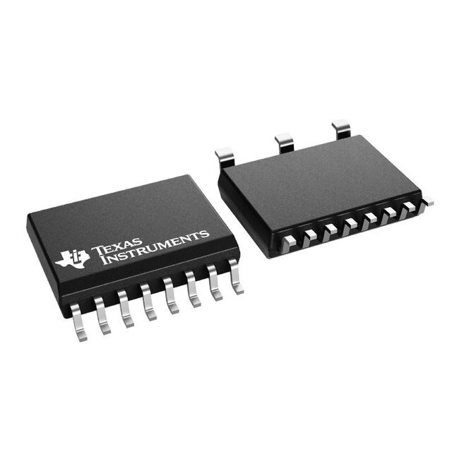
TPSI2140QDWQRQ1
ActiveAUTOMOTIVE 1200-V 50-MA ISOLATED SWITCH WITH 2-MA AVALANCHE RATING
Deep-Dive with AI
Search across all available documentation for this part.

TPSI2140QDWQRQ1
ActiveAUTOMOTIVE 1200-V 50-MA ISOLATED SWITCH WITH 2-MA AVALANCHE RATING
Deep-Dive with AI
Technical Specifications
Parameters and characteristics for this part
| Specification | TPSI2140QDWQRQ1 |
|---|---|
| Approval Agency | UL, CSA, CQC, TUV, VDE |
| Circuit | DPST-NO (2 Form A) |
| Grade | Automotive |
| Load Current | 50 mA |
| Mounting Type | Surface Mount |
| On-State Resistance (Max) [Max] | 300 Ohm |
| Operating Temperature [Max] | 125 °C |
| Operating Temperature [Min] | -40 C |
| Output Type | DC |
| Package / Case | 0.295 " |
| Package / Case | 11-SOIC |
| Package / Case [y] | 7.5 mm |
| Qualification | AEC-Q100 |
| Supplier Device Package | 11-SOIC |
| Termination Style | Gull Wing |
| Voltage - Input [Max] | 20 V |
| Voltage - Input [Min] | 4.5 V |
| Voltage - Load [Max] | 1200 V |
| Voltage - Load [Min] | 0 V |
Pricing
Prices provided here are for design reference only. For realtime values and availability, please visit the distributors directly
| Distributor | Package | Quantity | $ | |
|---|---|---|---|---|
| Digikey | Cut Tape (CT) | 1 | $ 6.61 | |
| 10 | $ 5.97 | |||
| 25 | $ 5.69 | |||
| 100 | $ 4.94 | |||
| 250 | $ 4.72 | |||
| 500 | $ 4.31 | |||
| 1000 | $ 3.75 | |||
| Digi-Reel® | 1 | $ 6.61 | ||
| 10 | $ 5.97 | |||
| 25 | $ 5.69 | |||
| 100 | $ 4.94 | |||
| 250 | $ 4.72 | |||
| 500 | $ 4.31 | |||
| 1000 | $ 3.75 | |||
| N/A | 4056 | $ 6.52 | ||
| Tape & Reel (TR) | 2000 | $ 3.61 | ||
| Texas Instruments | LARGE T&R | 1 | $ 4.02 | |
| 100 | $ 3.52 | |||
| 250 | $ 2.47 | |||
| 1000 | $ 1.99 | |||
Description
General part information
TPSI2140-Q1 Series
The TPSI2140-Q1 is an isolated solid state relay designed for high voltage automotive and industrial applications. The TPSI2140-Q1 uses TI’s high reliability capacitive isolation technology in combination with internal back-to-back MOSFETs to form a completely integrated solution requiring no secondary side power supply.
The primary side of the device is powered by only 9 mA of input current and incorporates a fail-safe EN pin preventing any possibility of back powering the VDD supply. In most applications, the VDD pin of the device should be connected to a system supply between 5 V–20 V and the EN pin of the device should be driven by a GPIO output with logic HI between 2.1 V–20 V. In other applications, The VDD and EN pins could be driven together directly from the system supply or from a GPIO output. All control configurations of the TPSI2140-Q1 do not require additional external components such as a resistor and/or low side switch that are typically required in photo relay solutions.
The secondary side consists of back-to-back MOSFETs with a standoff voltage of ±1.2 kV from S1 to S2. The TPSI2140-Q1 MOSFET’s avalanche robustness and thermally conscious package design allow it to robustly support system level dielectric withstand testing (HiPot) and DC fast charger surge currents of up to 2 mA without requiring any external components.
Documents
Technical documentation and resources


