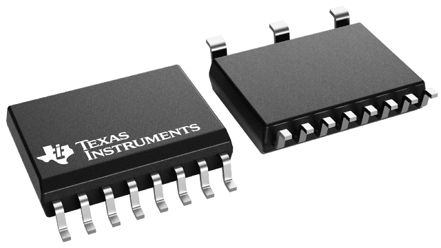
TPSI2140-Q1 Series
Automotive 1200-V 50-mA isolated switch with 2-mA avalanche rating
Manufacturer: Texas Instruments
Catalog
Automotive 1200-V 50-mA isolated switch with 2-mA avalanche rating
Description
AI
The TPSI2140-Q1 is an isolated solid state relay designed for high voltage automotive and industrial applications. The TPSI2140-Q1 uses TI’s high reliability capacitive isolation technology in combination with internal back-to-back MOSFETs to form a completely integrated solution requiring no secondary side power supply.
The primary side of the device is powered by only 9 mA of input current and incorporates a fail-safe EN pin preventing any possibility of back powering the VDD supply. In most applications, the VDD pin of the device should be connected to a system supply between 5 V–20 V and the EN pin of the device should be driven by a GPIO output with logic HI between 2.1 V–20 V. In other applications, The VDD and EN pins could be driven together directly from the system supply or from a GPIO output. All control configurations of the TPSI2140-Q1 do not require additional external components such as a resistor and/or low side switch that are typically required in photo relay solutions.
The secondary side consists of back-to-back MOSFETs with a standoff voltage of ±1.2 kV from S1 to S2. The TPSI2140-Q1 MOSFET’s avalanche robustness and thermally conscious package design allow it to robustly support system level dielectric withstand testing (HiPot) and DC fast charger surge currents of up to 2 mA without requiring any external components.


