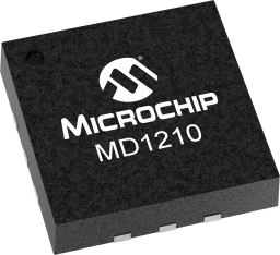
MD1210K6-G
ActiveHIGH SPEED DUAL MOSFET DRIVER 12 QFN 4X4X0.9MM T/R ROHS COMPLIANT: YES
Deep-Dive with AI
Search across all available documentation for this part.

MD1210K6-G
ActiveHIGH SPEED DUAL MOSFET DRIVER 12 QFN 4X4X0.9MM T/R ROHS COMPLIANT: YES
Deep-Dive with AI
Technical Specifications
Parameters and characteristics for this part
| Specification | MD1210K6-G |
|---|---|
| Channel Type | Independent |
| Current - Peak Output (Source, Sink) [custom] | 2 A |
| Current - Peak Output (Source, Sink) [custom] | 2 A |
| Driven Configuration | Half-Bridge |
| Gate Type | N-Channel, P-Channel MOSFET |
| Input Type | Non-Inverting |
| Logic Voltage - VIL, VIH | 0.3 V, 1.2 V |
| Mounting Type | Surface Mount |
| Number of Drivers | 2 |
| Operating Temperature [Max] | 125 ¯C |
| Operating Temperature [Min] | -20 °C |
| Package / Case | 12-VQFN Exposed Pad |
| Rise / Fall Time (Typ) [custom] | 6 ns |
| Rise / Fall Time (Typ) [custom] | 6 ns |
| Supplier Device Package | 12-QFN (4x4) |
| Voltage - Supply [Max] | 13 V |
| Voltage - Supply [Min] | 4.5 V |
Pricing
Prices provided here are for design reference only. For realtime values and availability, please visit the distributors directly
| Distributor | Package | Quantity | $ | |
|---|---|---|---|---|
| Digikey | Cut Tape (CT) | 1 | $ 2.01 | |
| 25 | $ 1.67 | |||
| 100 | $ 1.61 | |||
| Digi-Reel® | 1 | $ 2.01 | ||
| 25 | $ 1.67 | |||
| 100 | $ 1.61 | |||
| Tape & Reel (TR) | 5000 | $ 1.61 | ||
| Microchip Direct | T/R | 1 | $ 2.01 | |
| 25 | $ 1.67 | |||
| 100 | $ 1.52 | |||
| 1000 | $ 1.47 | |||
| 5000 | $ 1.45 | |||
| Newark | Each (Supplied on Full Reel) | 100 | $ 1.57 | |
Description
General part information
MD1210 Series
MD1210 is a high speed, dual MOSFET driver. It is designed to drive high voltage P and N-channel MOSFET transistors for medical ultrasound and other applications requiring a high output current for a capacitive load. The high-speed input stage of the MD1210 can operate from 1.2V to 5.0V logic interface with an optimum operating input signal range of 1.8V to 3.3V. An adaptive threshold circuit is used to set the level translator switch threshold to the average of the input logic 0 and logic 1 levels. The input logic levels may be ground referenced, even though the driver is putting out bipolar signals. The level translator uses a proprietary circuit, which provides DC coupling together with high-speed operation.
VDD1, VDD2, and VH should be connected to the positive supply voltage, and VSS1, VSS2, and VL should be connected to 0V or to Ground. The GND pin is the logic control input signal digital ground. The output stage is capable of peak currents of up to ±2.0A, depending on the supply voltages used and load capacitance present.
The OE pin serves a dual purpose. First, its logic H level is used to compute the threshold voltage level for the channel input level translators. Secondly, when OE is low, the outputs are disabled, with the A output high and the B output low. This assists in properly pre-charging the AC coupling capacitors that may be used in series in the gate drive circuit of an external PMOS and NMOS transistor pair.
Documents
Technical documentation and resources


