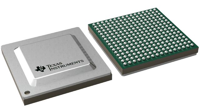
ADC12DL500ACF
Active12-BIT, DUAL 500MSPS OR SINGLE 1GSPS ANALOG-TO-DIGITAL CONVERTER (LVDS INTERFACE)
Deep-Dive with AI
Search across all available documentation for this part.

ADC12DL500ACF
Active12-BIT, DUAL 500MSPS OR SINGLE 1GSPS ANALOG-TO-DIGITAL CONVERTER (LVDS INTERFACE)
Technical Specifications
Parameters and characteristics for this part
| Specification | ADC12DL500ACF |
|---|---|
| Architecture | Folding Interpolating |
| Configuration | MUX-ADC |
| Data Interface | LVDS - Parallel |
| Input Type | Single Ended, Differential |
| Mounting Type | Surface Mount |
| Number of A/D Converters | 2 |
| Number of Bits | 12 bits |
| Number of Inputs | 1, 2 |
| Operating Temperature [Max] | 85 °C |
| Operating Temperature [Min] | -40 °C |
| Package / Case | 256-BBGA, FCBGA |
| Ratio - S/H:ADC | 0:2 |
| Reference Type | Internal |
| Sampling Rate (Per Second) | 1 G |
| Supplier Device Package | 256-FCBGA (17x17) |
| Voltage - Supply, Analog [Max] | 2 V, 1.15 V |
| Voltage - Supply, Analog [Min] | 1.8 V, 1.05 V |
| Voltage - Supply, Digital [Max] | 1.15 V |
| Voltage - Supply, Digital [Min] | 1.05 V |
Pricing
Prices provided here are for design reference only. For realtime values and availability, please visit the distributors directly
| Distributor | Package | Quantity | $ | |
|---|---|---|---|---|
| Digikey | Tube | 1 | $ 145.00 | |
| 10 | $ 138.14 | |||
| Texas Instruments | JEDEC TRAY (5+1) | 1 | $ 129.01 | |
| 100 | $ 125.13 | |||
| 250 | $ 104.18 | |||
| 1000 | $ 97.00 | |||
Description
General part information
ADC12DL500 Series
The ADC12DL500, ADC12DL1500 and ADC12DL2500 are a family of analog-to-digital converters (ADC) that can sample up to 500MSPS, 1.5GSPS, and 2.5GSPS in dual-channel mode and up to 1GSPS, 3GSPS, and 5GSPS in single-channel mode. Programmable tradeoffs in channel count (dual-channel mode) and sample rate (single-channel mode) allow development of flexible hardware that meets the needs of both high-channel count or wide instantaneous signal bandwidth applications.
The devices uses a low-latency, low-voltage differential signaling (LVDS) interface for latency sensitive applications or when the simplicity of LVDS is preferred. The interface uses up to 48 data pairs, four double data rate (DDR) clocks, and four strobe signals arranged in four 12-bit data buses. The interface supports signaling rates of up to 1.6Gbps. Strobe signals simplify synchronization across buses and between multiple devices. The strobe is generated internally and can be reset at a deterministic time by the SYSREF input. Multi-device synchronization is further eased by innovative synchronization features such as noiseless aperture delay (TAD) adjustment and SYSREF windowing.
The ADC12DL500, ADC12DL1500 and ADC12DL2500 are a family of analog-to-digital converters (ADC) that can sample up to 500MSPS, 1.5GSPS, and 2.5GSPS in dual-channel mode and up to 1GSPS, 3GSPS, and 5GSPS in single-channel mode. Programmable tradeoffs in channel count (dual-channel mode) and sample rate (single-channel mode) allow development of flexible hardware that meets the needs of both high-channel count or wide instantaneous signal bandwidth applications.
Documents
Technical documentation and resources


