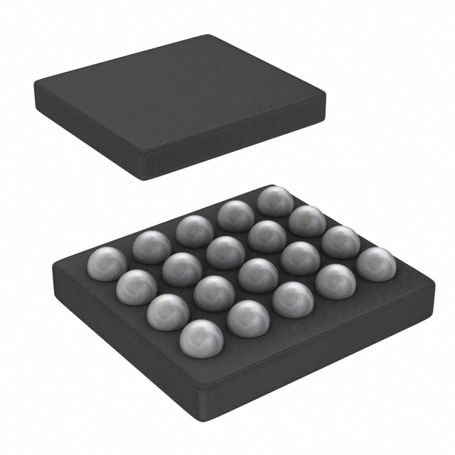
TPS630250YFFR
ActiveCONV DC-DC 2.3V TO 5.5V STEP DOWN/STEP UP SINGLE-OUT 2.3V TO 3.6V 2A 20-PIN DSBGA T/R
Deep-Dive with AI
Search across all available documentation for this part.

TPS630250YFFR
ActiveCONV DC-DC 2.3V TO 5.5V STEP DOWN/STEP UP SINGLE-OUT 2.3V TO 3.6V 2A 20-PIN DSBGA T/R
Deep-Dive with AI
Technical Specifications
Parameters and characteristics for this part
| Specification | TPS630250YFFR |
|---|---|
| Current - Output | 2 A, 4 A |
| Frequency - Switching | 2.5 MHz |
| Function | Step-Up/Step-Down |
| Mounting Type | Surface Mount |
| Number of Outputs | 1 |
| Operating Temperature [Max] | 85 C |
| Operating Temperature [Min] | -40 ¯C |
| Output Configuration | Positive |
| Output Type | Adjustable |
| Package / Case | 20-UFBGA, DSBGA |
| Supplier Device Package | 20-DSBGA |
| Synchronous Rectifier | True |
| Topology | Buck-Boost |
| Voltage - Input (Max) [Max] | 5.5 V |
| Voltage - Input (Min) [Min] | 2.3 V |
| Voltage - Output (Max) [Max] | 3.6 V |
| Voltage - Output (Min/Fixed) | 2.3 V |
Pricing
Prices provided here are for design reference only. For realtime values and availability, please visit the distributors directly
| Distributor | Package | Quantity | $ | |
|---|---|---|---|---|
| Digikey | Cut Tape (CT) | 1 | $ 2.38 | |
| 10 | $ 2.14 | |||
| 25 | $ 2.02 | |||
| 100 | $ 1.72 | |||
| 250 | $ 1.62 | |||
| 500 | $ 1.41 | |||
| 1000 | $ 1.17 | |||
| Digi-Reel® | 1 | $ 2.38 | ||
| 10 | $ 2.14 | |||
| 25 | $ 2.02 | |||
| 100 | $ 1.72 | |||
| 250 | $ 1.62 | |||
| 500 | $ 1.41 | |||
| 1000 | $ 1.17 | |||
| N/A | 3205 | $ 2.44 | ||
| Tape & Reel (TR) | 3000 | $ 1.09 | ||
| 6000 | $ 1.05 | |||
| Texas Instruments | LARGE T&R | 1 | $ 1.79 | |
| 100 | $ 1.48 | |||
| 250 | $ 1.06 | |||
| 1000 | $ 0.80 | |||
Description
General part information
TPS630250 Series
The TPS63025x are high efficiency, low quiescent current buck-boost converters suitable for application where the input voltage is higher or lower than the output. Output currents can go as high as 2 A in boost mode and as high as 4 A in buck mode. The maximum average current in the switches is limited to a typical value of 4 A. The TPS63025x regulates the output voltage over the complete input voltage range by automatically switching between buck or boost mode depending on the input voltage ensuring a seamless transition between modes. The buck-boost converter is based on a fixed frequency, pulse-width-modulation (PWM) controller using synchronous rectification to obtain highest efficiency. At low load currents, the converter enters Power Save Mode to maintain high efficiency over the complete load current range. There is a PFM/PWM pin that allows the user to choose between automatic PFM/PWM mode operation and forced PWM operation. During PWM mode a fixed-frequency of typically 2.5 MHz is used. The output voltage is programmable using an external resistor divider, or is fixed internally on the chip. The converter can be disabled to minimize battery drain. During shutdown, the load is disconnected from the battery. The device is packaged in a 20-pin WCSP package measuring 1.766 mm × 2.086mm and 14-pin HotRod package measuring 2.5 mm × 3mm.
The TPS63025x are high efficiency, low quiescent current buck-boost converters suitable for application where the input voltage is higher or lower than the output. Output currents can go as high as 2 A in boost mode and as high as 4 A in buck mode. The maximum average current in the switches is limited to a typical value of 4 A. The TPS63025x regulates the output voltage over the complete input voltage range by automatically switching between buck or boost mode depending on the input voltage ensuring a seamless transition between modes. The buck-boost converter is based on a fixed frequency, pulse-width-modulation (PWM) controller using synchronous rectification to obtain highest efficiency. At low load currents, the converter enters Power Save Mode to maintain high efficiency over the complete load current range. There is a PFM/PWM pin that allows the user to choose between automatic PFM/PWM mode operation and forced PWM operation. During PWM mode a fixed-frequency of typically 2.5 MHz is used. The output voltage is programmable using an external resistor divider, or is fixed internally on the chip. The converter can be disabled to minimize battery drain. During shutdown, the load is disconnected from the battery. The device is packaged in a 20-pin WCSP package measuring 1.766 mm × 2.086mm and 14-pin HotRod package measuring 2.5 mm × 3mm.
Documents
Technical documentation and resources


