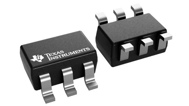
CLVC1G175MDCKREP
ActiveENHANCED PRODUCT SINGLE D-TYPE FLIP-FLOP WITH ASYNCHRONOUS CLEAR
Deep-Dive with AI
Search across all available documentation for this part.

CLVC1G175MDCKREP
ActiveENHANCED PRODUCT SINGLE D-TYPE FLIP-FLOP WITH ASYNCHRONOUS CLEAR
Technical Specifications
Parameters and characteristics for this part
| Specification | CLVC1G175MDCKREP |
|---|---|
| Current - Output High, Low [x] | 32 mA |
| Current - Output High, Low [y] | 32 mA |
| Current - Quiescent (Iq) | 10 µA |
| Function | Reset |
| Input Capacitance | 3 pF |
| Max Propagation Delay @ V, Max CL | 5 ns |
| Mounting Type | Surface Mount |
| Number of Bits per Element | 1 |
| Number of Elements | 1 |
| Operating Temperature [Max] | 125 °C |
| Operating Temperature [Min] | -55 °C |
| Output Type | Non-Inverted |
| Package / Case | 6-TSSOP, SC-88, SOT-363 |
| Supplier Device Package | SC-70-6 |
| Trigger Type | Positive Edge |
| Type | D-Type |
| Voltage - Supply [Max] | 5.5 V |
| Voltage - Supply [Min] | 1.65 V |
Pricing
Prices provided here are for design reference only. For realtime values and availability, please visit the distributors directly
| Distributor | Package | Quantity | $ | |
|---|---|---|---|---|
| Digikey | Cut Tape (CT) | 1 | $ 2.83 | |
| 10 | $ 1.83 | |||
| 25 | $ 1.57 | |||
| 100 | $ 1.28 | |||
| 250 | $ 1.13 | |||
| 500 | $ 1.05 | |||
| 1000 | $ 0.97 | |||
| Digi-Reel® | 1 | $ 2.83 | ||
| 10 | $ 1.83 | |||
| 25 | $ 1.57 | |||
| 100 | $ 1.28 | |||
| 250 | $ 1.13 | |||
| 500 | $ 1.05 | |||
| 1000 | $ 0.97 | |||
| Tape & Reel (TR) | 3000 | $ 0.88 | ||
| 6000 | $ 0.84 | |||
| 9000 | $ 0.82 | |||
| Texas Instruments | LARGE T&R | 1 | $ 1.65 | |
| 100 | $ 1.36 | |||
| 250 | $ 0.98 | |||
| 1000 | $ 0.74 | |||
Description
General part information
SN74LVC1G175-EP Series
This single D-type flip-flop is designed for 1.65-V to 5.5-V VCCoperation.
The SN74LVC1G175 has an asynchronous clear (CLR) input. WhenCLRis high, data from the input pin (D) is transferred to the output pin (Q) on the clock’s (CLK) rising edge. WhenCLRis low, Q is forced into the low state, regardless of the clock edge or data on D.
This device is fully specified for partial-power-down applications using Ioff. The Ioffcircuitry disables the outputs, preventing damaging current backflow through the device when it is powered down.
Documents
Technical documentation and resources


