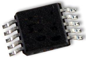
AD4001BRMZ
ActiveANALOG TO DIGITAL CONVERTER, 16 BIT, 2 MSPS, DIFFERENTIAL, MICROWIRE, QSPI, SPI, SINGLE, 1.71 V
Deep-Dive with AI
Search across all available documentation for this part.

AD4001BRMZ
ActiveANALOG TO DIGITAL CONVERTER, 16 BIT, 2 MSPS, DIFFERENTIAL, MICROWIRE, QSPI, SPI, SINGLE, 1.71 V
Technical Specifications
Parameters and characteristics for this part
| Specification | AD4001BRMZ |
|---|---|
| Architecture | SAR |
| Configuration | S/H-ADC |
| Data Interface | DSP, SPI |
| Input Type | Differential |
| Mounting Type | Surface Mount |
| Number of A/D Converters | 1 |
| Number of Bits | 16 |
| Number of Inputs | 1 |
| Operating Temperature [Max] | 125 °C |
| Operating Temperature [Min] | -40 °C |
| Package / Case | 10-MSOP, 10-TFSOP |
| Package / Case [x] | 3 mm |
| Package / Case [x] | 0.118 in |
| Ratio - S/H:ADC | 1:1 |
| Reference Type | External |
| Sampling Rate (Per Second) | 2M |
| Supplier Device Package | 10-MSOP |
| Voltage - Supply, Analog [Max] | 1.89 V |
| Voltage - Supply, Analog [Min] | 1.71 V |
| Voltage - Supply, Digital [Max] | 5.5 V |
| Voltage - Supply, Digital [Min] | 1.71 V |
Pricing
Prices provided here are for design reference only. For realtime values and availability, please visit the distributors directly
Description
General part information
AD4001 Series
The AD4001/AD4005 are high accuracy, high speed, low power, 16-bit, Easy Drive, precision successive approximation register (SAR) analog-to-digital converters (ADCs) that operate from a single power supply, VDD. The reference voltage, VREF, is applied externally and can be set independent of the supply voltage. The AD4001/AD4005 power scales linearly with throughput.Easy Drive features reduce both signal chain complexity and power consumption while enabling higher channel density. The reduced input current, particularly in high-Z mode, coupled with a long signal acquisition phase, eliminates the need for a dedicated ADC driver. Easy Drive broadens the range of companion circuitry that is capable of driving these ADCs (see Figure 2 in the data sheet).Input span compression eliminates the need to provide a negative supply to the ADC driver amplifier while preserving access to the full ADC code range. The input overvoltage clamp protects the ADC inputs against overvoltage events, minimizing disturbances on the reference pin and eliminating the need for external protection diodes.Fast device throughput up to 2 MSPS allows users to accurately capture high frequency signals and to implement oversampling techniques to alleviate the challenges associated with antialias filter designs. Decreased serial peripheral interface (SPI) clock rate requirements reduce digital input and output power consumption, broadens digital host options, and simplifies the task of sending data across digital isolation. The SPI-compatible serial user interface is compatible with 1.8 V, 2.5 V, 3 V, and 5 V logic by using the separate VIO logic supply.APPLICATIONSAutomated test equipmentMachine automationMedical equipmentBattery-powered equipmentPrecision data acquisition systemsInstrumentation and control systems
Documents
Technical documentation and resources


