Deep-Dive with AI
Search across all available documentation for this part.

Deep-Dive with AI
Technical Specifications
Parameters and characteristics for this part
| Specification | SN74LV374ATDWR |
|---|---|
| Clock Frequency | 150 MHz |
| Current - Output High, Low [custom] | 16 mA |
| Current - Output High, Low [custom] | 16 mA |
| Current - Quiescent (Iq) | 2 µA |
| Function | Standard |
| Input Capacitance | 4 pF |
| Max Propagation Delay @ V, Max CL | 10.1 ns |
| Mounting Type | Surface Mount |
| Number of Bits per Element | 8 |
| Number of Elements | 1 |
| Operating Temperature [Max] | 125 °C |
| Operating Temperature [Min] | -40 °C |
| Output Type | Tri-State, Non-Inverted |
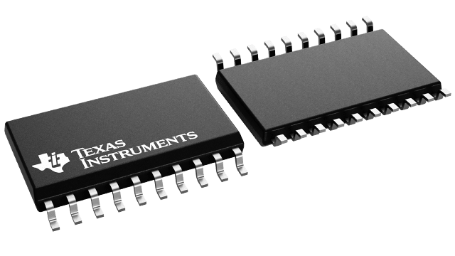
| Package / Case | 20-SOIC |
| Package / Case [y] | 0.295 in |
| Package / Case [y] | 7.5 mm |
| Supplier Device Package | 20-SOIC |
| Trigger Type | Positive Edge |
| Type | D-Type |
| Voltage - Supply [Max] | 5.5 V |
| Voltage - Supply [Min] | 4.5 V |
Pricing
Prices provided here are for design reference only. For realtime values and availability, please visit the distributors directly
| Distributor | Package | Quantity | $ | |
|---|---|---|---|---|
| Digikey | Cut Tape (CT) | 1 | $ 0.67 | |
| 10 | $ 0.59 | |||
| 25 | $ 0.55 | |||
| 100 | $ 0.45 | |||
| 250 | $ 0.42 | |||
| 500 | $ 0.36 | |||
| 1000 | $ 0.29 | |||
| Digi-Reel® | 1 | $ 0.67 | ||
| 10 | $ 0.59 | |||
| 25 | $ 0.55 | |||
| 100 | $ 0.45 | |||
| 250 | $ 0.42 | |||
| 500 | $ 0.36 | |||
| 1000 | $ 0.29 | |||
| Tape & Reel (TR) | 2000 | $ 0.26 | ||
| 6000 | $ 0.24 | |||
| 10000 | $ 0.23 | |||
| Texas Instruments | LARGE T&R | 1 | $ 0.58 | |
| 100 | $ 0.40 | |||
| 250 | $ 0.31 | |||
| 1000 | $ 0.20 | |||
Description
General part information
SN74LV374A-EP Series
The SN74LV374A is an octal edge-triggered D-type flip-flop designed for 2-V to 5.5-V VCCoperation.
This device features 3-state outputs designed specifically for driving highly capacitive or relatively low-impedance loads. It is particularly suitable for implementing buffer registers, I/O ports, bidirectional bus drivers, and working registers.
On the positive transition of the clock (CLK) input, the Q outputs are set to the logic levels set up at the data (D) inputs.
Documents
Technical documentation and resources


