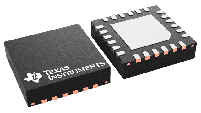
CDCI6214RGET
NRNDPCIE GEN4 SUPPORT ULTRA-LOW POWER CLOCK GENERATOR WITH FOUR PROGRAMMABLE OUTPUTS & EEPROM
Deep-Dive with AI
Search across all available documentation for this part.

CDCI6214RGET
NRNDPCIE GEN4 SUPPORT ULTRA-LOW POWER CLOCK GENERATOR WITH FOUR PROGRAMMABLE OUTPUTS & EEPROM
Technical Specifications
Parameters and characteristics for this part
| Specification | CDCI6214RGET |
|---|---|
| Differential - Input:Output [custom] | True |
| Differential - Input:Output [custom] | True |
| Divider/Multiplier | False |
| Frequency - Max [Max] | 250 MHz |
| Input | LVCMOS, Crystal |
| Mounting Type | Surface Mount |
| Number of Circuits | 2 |
| Operating Temperature [Max] | 85 °C |
| Operating Temperature [Min] | -40 °C |
| Output | LVCMOS, LVDS, HCSL |
| Package / Case | 24-VFQFN Exposed Pad |
| PLL | Yes with Bypass |
| Ratio - Input:Output | 1:5 |
| Supplier Device Package | 24-VQFN (4x4) |
| Type | Clock Generator |
| Voltage - Supply [Max] | 3.465 V |
| Voltage - Supply [Min] | 1.71 V |
Pricing
Prices provided here are for design reference only. For realtime values and availability, please visit the distributors directly
| Distributor | Package | Quantity | $ | |
|---|---|---|---|---|
| Digikey | Cut Tape (CT) | 1 | $ 12.03 | |
| 10 | $ 11.05 | |||
| 25 | $ 10.59 | |||
| 100 | $ 9.33 | |||
| Digi-Reel® | 1 | $ 12.03 | ||
| 10 | $ 11.05 | |||
| 25 | $ 10.59 | |||
| 100 | $ 9.33 | |||
| Tape & Reel (TR) | 250 | $ 3.30 | ||
| Texas Instruments | SMALL T&R | 1 | $ 12.00 | |
| 100 | $ 9.78 | |||
| 250 | $ 7.69 | |||
| 1000 | $ 6.52 | |||
Description
General part information
CDCI6214 Series
The CDCI6214 device is an ultra-low power clock generator. The device selects between two independent reference inputs to a phase-locked loop and generates up to four different frequencies on configurable differential output channels and also a copy of the reference clock on a LVCMOS output channel.
Each of the four output channels has a configurable integer divider. Together with the output muxes, this allows up to five different frequencies. Clock distribution dividers are reset in a deterministic way for clean clock gating and glitch-less update capability. Flexible power-down options allow to optimize the device for lowest power consumption in active and standby operation. Typically four 156.25MHz LVDS outputs consume 150mW at 1.8V. Typical RMS jitter of 386fs for 100MHz HCSL output enhances system margin for PCIe applications.
The CDCI6214 is configured using internal registers that are accessed by an I2C-compatible serial interface and internal EEPROM.
Documents
Technical documentation and resources


