CDCI6214 Series
PCIe Gen4 support ultra-low power clock generator with four programmable outputs & EEPROM
Manufacturer: Texas Instruments
Catalog
PCIe Gen4 support ultra-low power clock generator with four programmable outputs & EEPROM
Key Features
• One configurable high performance, low-power PLL with four programmable outputsRMS jitter performanceSupports PCIe Gen1/ Gen2 / Gen3 / Gen4 without SSCTypical power consumption: 150mW at 1.8V(2)Universal clock inputDifferential AC-coupled or LVCMOS: 1MHz to 250MHzCrystal: 8MHz to 50MHzFlexible output frequencies44.1kHz to 350MHzGlitchless output divider switchingFour individually configurable outputsLVCMOS, LVDS or HCSLDifferential AC-coupled with programmable swing (LVDS-, CML-, LVPECL-compatible)Fully integrated PLL, configurable loop bandwidth: 100kHz to 3MHzSingle or mixed supply operation for level translation: 1.8V, 2.5V and 3.3VConfigurable GPIOsStatus signalsUp to four individual output enablesOutput divider synchronizationFlexible configuration optionsI2C-compatible interface: up to 400kHzIntegrated EEPROM with two pages and external select pinOnly supports 100Ω systemsIndustrial temperature range: –40°C to 85°CSmall footprint: 24-pin VQFN (4mm × 4mm)One configurable high performance, low-power PLL with four programmable outputsRMS jitter performanceSupports PCIe Gen1/ Gen2 / Gen3 / Gen4 without SSCTypical power consumption: 150mW at 1.8V(2)Universal clock inputDifferential AC-coupled or LVCMOS: 1MHz to 250MHzCrystal: 8MHz to 50MHzFlexible output frequencies44.1kHz to 350MHzGlitchless output divider switchingFour individually configurable outputsLVCMOS, LVDS or HCSLDifferential AC-coupled with programmable swing (LVDS-, CML-, LVPECL-compatible)Fully integrated PLL, configurable loop bandwidth: 100kHz to 3MHzSingle or mixed supply operation for level translation: 1.8V, 2.5V and 3.3VConfigurable GPIOsStatus signalsUp to four individual output enablesOutput divider synchronizationFlexible configuration optionsI2C-compatible interface: up to 400kHzIntegrated EEPROM with two pages and external select pinOnly supports 100Ω systemsIndustrial temperature range: –40°C to 85°CSmall footprint: 24-pin VQFN (4mm × 4mm)
Description
AI
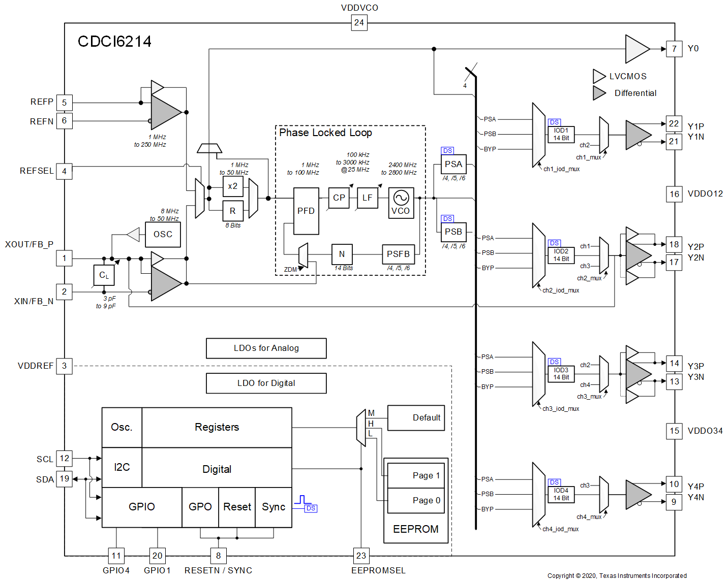
The CDCI6214 device is an ultra-low power clock generator. The device selects between two independent reference inputs to a phase-locked loop and generates up to four different frequencies on configurable differential output channels and also a copy of the reference clock on a LVCMOS output channel.
Each of the four output channels has a configurable integer divider. Together with the output muxes, this allows up to five different frequencies. Clock distribution dividers are reset in a deterministic way for clean clock gating and glitch-less update capability. Flexible power-down options allow to optimize the device for lowest power consumption in active and standby operation. Typically four 156.25MHz LVDS outputs consume 150mW at 1.8V. Typical RMS jitter of 386fs for 100MHz HCSL output enhances system margin for PCIe applications.
The CDCI6214 is configured using internal registers that are accessed by an I2C-compatible serial interface and internal EEPROM.
The CDCI6214 enables high-performance clock trees from a single reference at ultra-low power with a small footprint. The factory- and user-programmable EEPROM of the CDCI6214 is designed as an easy-to-use, instant-on clocking feature with low power consumption.


