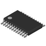
MAX5318GUG+T
Active18-BIT, HIGH-ACCURACY VOLTAGE OUTPUT DAC WITH DIGITAL GAIN, OFFSET CONTROL, AND SPI INTERFACE
Deep-Dive with AI
Search across all available documentation for this part.

MAX5318GUG+T
Active18-BIT, HIGH-ACCURACY VOLTAGE OUTPUT DAC WITH DIGITAL GAIN, OFFSET CONTROL, AND SPI INTERFACE
Deep-Dive with AI
Technical Specifications
Parameters and characteristics for this part
| Specification | MAX5318GUG+T |
|---|---|
| Data Interface | SPI |
| Differential Output | False |
| INL/DNL (LSB) | 0.75 LSB, 0.3 LSB |
| Mounting Type | Surface Mount |
| Number of D/A Converters | 1 |
| Operating Temperature [Max] | 105 ░C |
| Operating Temperature [Min] | -40 C |
| Output Type | Voltage - Buffered |
| Package / Case | 24-TSSOP |
| Package / Case [x] | 4.4 mm |
| Package / Case [x] | 0.173 in |
| Reference Type | External |
| Settling Time | 3 µs |
| Supplier Device Package | 24-TSSOP |
| Voltage - Supply, Analog | 5 V, -1.25 V |
| Voltage - Supply, Analog [Max] | 3.3 V |
| Voltage - Supply, Analog [Min] | 2.7 V |
Pricing
Prices provided here are for design reference only. For realtime values and availability, please visit the distributors directly
Description
General part information
MAX5318 Series
The MAX5318 is a high-accuracy, 18-bit, serial SPI input, buffered voltage output digital-to-analog converter (DAC) in a 4.4mm x 7.8mm, 24-lead TSSOP package. The device features ±2 LSB INL (max) accuracy and a ±1 LSB DNL (max) accuracy over the full temperature range of -40°C to +105°C.The DAC voltage output is buffered resulting in a fast settling time of 3µs and a low offset and gain drift of ±0.5ppm/°C of FSR (typ). The force-sense output (OUT) maintains accuracy while driving loads with long lead lengths. Additionally, a separate AVSS supply, allows the output amplifier to go to 0V (GND) while maintaining full linearity performance.The MAX5318 includes user-programmable digital gain and offset correction to enable easy system calibration.At power-up, the device resets its outputs to zero or midscale. The wide 2.7V to 5.5V supply voltage range and integrated low-drift, low-noise reference buffer amplifier make for ease of use.The MAX5318 features a 50MHz, 3-wire, SPI interface. The MAX5318 is available in a 24-lead TSSOP package and operates over the -40°C to +105°C temperature range.ApplicationsAutomatic Test EquipmentAutomatic Tuning and CalibrationCommunication SystemsData-Acquisition SystemsGain and Offset AdjustmentMedical ImagingProcess Control and Servo LoopsProgrammable Voltage and Current SourcesTest and Measurement Equipment
Documents
Technical documentation and resources


