Deep-Dive with AI
Search across all available documentation for this part.

Deep-Dive with AI
Technical Specifications
Parameters and characteristics for this part
| Specification | AD7396AR-REEL |
|---|---|
| Architecture | R-2R |
| Data Interface | Parallel |
| Differential Output | False |
| INL/DNL (LSB) | ±2 (Max), ±1 (Max) |
| Mounting Type | Surface Mount |
| Number of Bits | 12 bits |
| Operating Temperature [Max] | 85 °C |
| Operating Temperature [Min] | -40 °C |
| Output Type | Voltage - Buffered |
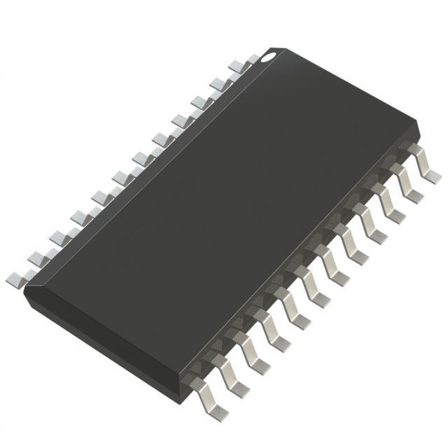
| Package / Case | 24-SOIC |
| Package / Case [custom] | 7.5 mm |
| Package / Case [custom] | 0.295 in |
| Reference Type | External |
| Settling Time | 70 µs |
| Supplier Device Package | 24-SOIC |
| Voltage - Supply, Analog [Max] | 5.5 V |
| Voltage - Supply, Analog [Min] | 2.7 V |
| Voltage - Supply, Digital [Max] | 5.5 V |
| Voltage - Supply, Digital [Min] | 2.7 V |
Pricing
Prices provided here are for design reference only. For realtime values and availability, please visit the distributors directly
| Distributor | Package | Quantity | $ | |
|---|---|---|---|---|
Description
General part information
AD7396 Series
The AD7396 /AD7397series of dual, pin-compatible, 12- and 10-bit voltage-output digital-to-analog converters save power while operating from +3 V to +5 V supplies. A unique feature of the high-input-resistance, reference inputs is the ability to tie VREFto VDDestablishing a full 0 to VDDDAC output swing. Operation is guaranteed over the supply voltage range of +2.7 V to +5.5 V making these devices ideal for battery-operated applications.A 12-bit wide latch loads with a 45 ns write time allowing interface to fast processors without wait states. The double-buffered input structure enables pre-load of the input registers one at a time, then a single load strobe tied to bothLDA+LDBinputs will update both DAC outputs simultaneously. Additionally, an asynchronousRSinput sets the output to zero-scale at power on or upon user demand. Power shutdown to sub microamp levels is directly controlled by the active lowSHDNpin. While in the power shutdown state register data can still be changed even though the output buffer is in an open circuit state. Upon return to the normal operating state the latest data loaded in the DAC register will establish the output voltage.Both parts are offered in the same pin out to allow users to select the amount of resolution appropriate for their applications without circuit card changes. Primary applications for the AD7396 / AD7397 include: automotive sensor voltage generation and calibration, portable communications, PC peripherals and digitally controlled calibration.The AD7396 and AD7397 are specified for operation over the extended industrial (-40°C to +85°C) temperature range. The AD7397AN and AD7397AR are specified for the -40°C to +125°C automotive temperature range. AD7396s and AD7397s are available in plastic DIP, and 24-lead SOIC packages. The AD7397ARU is available for ultra-compact applications for example, PCMCIA cards, in a thin 1.1mm height TSSOP-24 package.The AD7396 and AD7397 are members of a complete family of Micropower consumption, single/dual/quad D/A converters (AD7390 … AD7398) available with both serial or parallel data loading.
Documents
Technical documentation and resources


