Deep-Dive with AI
Search across all available documentation for this part.

Deep-Dive with AI
Technical Specifications
Parameters and characteristics for this part
| Specification | HV66PJ-G |
|---|---|
| Current - Supply | 15 mA |
| Display Type | LCD |
| Interface | Serial |
| Mounting Type | Surface Mount |
| Operating Temperature [Max] | 85 °C |
| Operating Temperature [Min] | -40 °C |
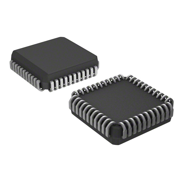
| Package / Case | 44-LCC (J-Lead) |
| Supplier Device Package | 44-PLCC (16.59x16.59) |
| Voltage - Supply [Max] | 5.5 V |
| Voltage - Supply [Min] | 4.5 V |
Pricing
Prices provided here are for design reference only. For realtime values and availability, please visit the distributors directly
| Distributor | Package | Quantity | $ | |
|---|---|---|---|---|
| Digikey | Tube | 1 | $ 4.00 | |
| 25 | $ 3.35 | |||
| 100 | $ 3.04 | |||
| Microchip Direct | CTUBE | 1 | $ 4.00 | |
| 25 | $ 3.35 | |||
| 100 | $ 3.04 | |||
| 1000 | $ 2.94 | |||
| 5000 | $ 2.91 | |||
Description
General part information
HV66 Series
The HV66 is a low voltage serial to high voltage parallel converter with push-pull outputs. This device has been designed for use as a driver circuit for LCD displays. It can also be used in any application requiring multiple output high voltage current sourcing and sinking capabilities. The inputs are fully CMOS compatible.
The device consists of a 32-bit shift register, 32 latches, and control logic to perform blanking and polarity control of the outputs. HVOUT1 is connected to the first stage of the shift register. Data is shifted through the shift register on the logic rising transition of the clock. A DIR pin causes data shifting clockwise when grounded and counter clockwise when connected to VDD. A data output buffer is provided for cascading devices. This output reflects the current status of the last bit of the shift register. Operation of the shift register is not affected by the LE (latch enable), BL (blank) or the POL (polarity) inputs. Transfer of data from the shift register to the latch occurs when the LE (latch enable) input is high. The data in the latch is stored after LE transitions from high to low.
Documents
Technical documentation and resources


