Deep-Dive with AI
Search across all available documentation for this part.

Deep-Dive with AI
Technical Specifications
Parameters and characteristics for this part
| Specification | AD7934BRU |
|---|---|
| Architecture | SAR |
| Configuration | MUX-S/H-ADC |
| Data Interface | Parallel |
| Input Type | Single Ended, Differential, Pseudo-Differential |
| Mounting Type | Surface Mount |
| Number of A/D Converters | 1 |
| Number of Bits | 12 bits |
| Number of Inputs | 4 |
| Operating Temperature [Max] | 85 °C |
| Operating Temperature [Min] | -40 °C |
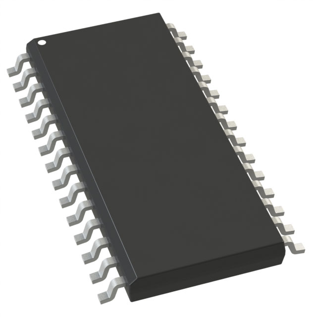
| Package / Case | 28-TSSOP |
| Package / Case | 0.173 in |
| Package / Case [y] | 4.4 mm |
| Ratio - S/H:ADC | 1:1 |
| Reference Type | External, Internal |
| Sampling Rate (Per Second) | 1.5 M |
| Supplier Device Package | 28-TSSOP |
| Voltage - Supply, Analog [Max] | 5.25 V |
| Voltage - Supply, Analog [Min] | 2.7 V |
| Voltage - Supply, Digital [Max] | 5.25 V |
| Voltage - Supply, Digital [Min] | 2.7 V |
Pricing
Prices provided here are for design reference only. For realtime values and availability, please visit the distributors directly
| Distributor | Package | Quantity | $ | |
|---|---|---|---|---|
Description
General part information
AD7934 Series
The AD7933/AD7934 are 10-bit and 12-bit, high speed, low power, successive approximation (SAR) analog-to-digital converters (ADCs). The parts operate from a single 2.7 V to 5.25 V power supply and feature throughput rates up to 1.5 MSPS. The parts contain a low noise, wide bandwidth, differential track-and-hold amplifier that handles input frequencies up to 50 MHz.The AD7933/AD7934 feature four analog input channels with a channel sequencer that allows a preprogrammed selection of channels to be sequentially converted. These parts can accept either single-ended, fully differential, or pseudo differential analog inputs.The conversion process and data acquisition are controlled using standard control inputs that allow for easy interfacing to microprocessors and DSPs. The input signal is sampled on the falling edge ofCONVST, and the conversion is also initiated at this point.The AD7933/AD7934 has an accurate on-chip 2.5 V reference that is used as the reference source for the analog-to-digital conversion. Alternatively, this pin can be overdriven to provide an external reference.These parts use advanced design techniques to achieve very low power dissipation at high throughput rates. They also feature flexible power management options. An on-chip control register allows the user to set up different operating conditions, including analog input range and configuration, output coding, power management, and channel sequencing.PRODUCT HIGHLIGHTSHigh throughput with low power consumption.Four analog inputs with a channel sequencer.Accurate on-chip 2.5 V reference.Single-ended, pseudo differential or fully differential analog inputs that are software selectable.Single-supply operation with VDRIVEfunction. The VDRIVEfunction allows the parallel interface to connect directly to 3 V or 5 V processor systems independent of VDD.No pipeline delay.Accurate control of the sampling instant via aCONVSTinput and once-off conversion control.
Documents
Technical documentation and resources


