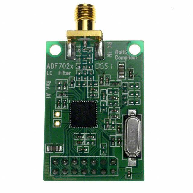
EVAL-ADF7020-1DBZ5
ActiveADF7020-1 RF TRANSCEIVER DAUGHTER BOARD
Deep-Dive with AI
Search across all available documentation for this part.

EVAL-ADF7020-1DBZ5
ActiveADF7020-1 RF TRANSCEIVER DAUGHTER BOARD
Deep-Dive with AI
Technical Specifications
Parameters and characteristics for this part
| Specification | EVAL-ADF7020-1DBZ5 |
|---|---|
| Contents | Board(s) |
| For Use With/Related Products | ADF7020-1 |
| Frequency [Max] | 650 MHz |
| Frequency [Min] | 80 MHz |
| Supplied Contents | Board(s) |
| Type | Transceiver, ASK |
| Utilized IC / Part | ADF7020-1 |
Pricing
Prices provided here are for design reference only. For realtime values and availability, please visit the distributors directly
| Distributor | Package | Quantity | $ | |
|---|---|---|---|---|
| Digikey | Box | 1 | $ 80.19 | |
Description
General part information
ADF7020-1 Series
The ADF7020-1 is a low power, highly integrated FSK/ GFSK/ ASK/ OOK/ GOOK transceiver designed for operation in the low UHF and VHF bands. The ADF7020-1 uses an external VCO inductor that allows users to set the operating frequency anywhere between 135 MHz and 650 MHz. Using the divide-by-2 circuit allows users to operate the device as low as 80 MHz. The typical range of the VCO is about 10% of the operating frequency. A complete transceiver can be built using a small number of external discrete components, making the ADF7020-1 very suitable for price-sensitive and area-sensitive applications.The transmit section contains a VCO and low noise fractional-N PLL with output resolution of <1 ppm. This frequency agile PLL allows the ADF7020-1 to be used in frequency-hopping spread spectrum (FHSS) systems. The VCO operates at twice the fundamental frequency to reduce spurious emissions and frequency pulling problems.The transmitter output power is programmable in 63 steps from −20 dBm to +13 dBm. The transceiver RF frequency, channel spacing, and modulation are programmable using a simple 3-wire interface. The device operates with a power supply range of 2.3 V to 3.6 V and can be powered down when not in useA low IF architecture is used in the receiver (200 kHz), minimizing power consumption and the external component count and avoiding interference problems at low frequencies. The ADF7020-1 supports a wide variety of programmable features, including Rx linearity, sensitivity, and IF bandwidth, allowing the user to trade off receiver sensitivity and selectivity for current consumption, depending on the application. The receiver also features a patent-pending automatic frequency control (AFC) loop, allowing the PLL to compensate for frequency error in the incoming signal.An on-chip ADC provides readback of an integrated temperature sensor, an external analog input, the battery voltage, or the RSSI signal, which provides savings on an ADC in some applications. The temperature sensor is accurate to ±10°C over the full operating temperature range of −40°C to +85°C. This accuracy can be improved by doing a 1-point calibration at room temperature and storing the result in memory.ApplicationsLow cost wireless data transferWireless medical applicationsRemote control/security systemsWireless meteringKeyless entryHome automationProcess and building control
Documents
Technical documentation and resources


