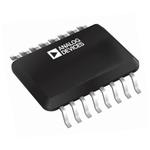
AD7888BRZ
Active2.7 V TO 5.25 V, MICRO POWER, 8-CHANNEL, 125 KSPS, 12-BIT ADC IN 16-PIN TSSOP
Deep-Dive with AI
Search across all available documentation for this part.

AD7888BRZ
Active2.7 V TO 5.25 V, MICRO POWER, 8-CHANNEL, 125 KSPS, 12-BIT ADC IN 16-PIN TSSOP
Deep-Dive with AI
Technical Specifications
Parameters and characteristics for this part
| Specification | AD7888BRZ |
|---|---|
| Architecture | SAR |
| Configuration | MUX-S/H-ADC |
| Data Interface | DSP, SPI |
| Input Type | Single Ended |
| Mounting Type | Surface Mount |
| Number of A/D Converters | 1 |
| Number of Bits | 12 bits |
| Number of Inputs | 8 |
| Operating Temperature [Max] | 105 ░C |
| Operating Temperature [Min] | -40 °C |
| Package / Case | 16-SOIC |
| Package / Case [x] | 0.154 in |
| Package / Case [y] | 3.9 mm |
| Ratio - S/H:ADC | 1:1 |
| Reference Type | External, Internal |
| Supplier Device Package | 16-SOIC |
| Voltage - Supply, Analog [Max] | 5.25 V |
| Voltage - Supply, Analog [Min] | 2.7 V |
| Voltage - Supply, Digital [Max] | 5.25 V |
| Voltage - Supply, Digital [Min] | 2.7 V |
Pricing
Prices provided here are for design reference only. For realtime values and availability, please visit the distributors directly
Description
General part information
AD7888 Series
The AD7888 is a high speed, low power, 12-bit ADC that operates from a single 2.7 V to 5.25 V power supply. The AD7888 is capable of a 125 kSPS throughput rate. The input track-and-hold acquires a signal in 500 ns and features a single ended sampling scheme. The AD7888 contains eight single-ended analog inputs, AIN1 through AIN8. The analog input on each of these channels is from 0 to VREF. The part is capable of converting full power signals up to 3 MHz.The AD7888 features an on-chip 2.5 V reference that can be used as the reference source for the A/D converter. The REF IN/REF OUT pin allows the user access to this reference. Alternatively, this pin can be overdriven to provide an external reference voltage for the AD7888. The voltage range for this external reference is from 1.2 V to VDD.CMOS construction ensures low power dissipation of typically 2 mW for normal operation and 3 µW in power-down mode. The part is available in a 16-lead narrow body small outline (SOIC) and a 16-lead thin small shrink outline (TSSOP) package.
Documents
Technical documentation and resources


