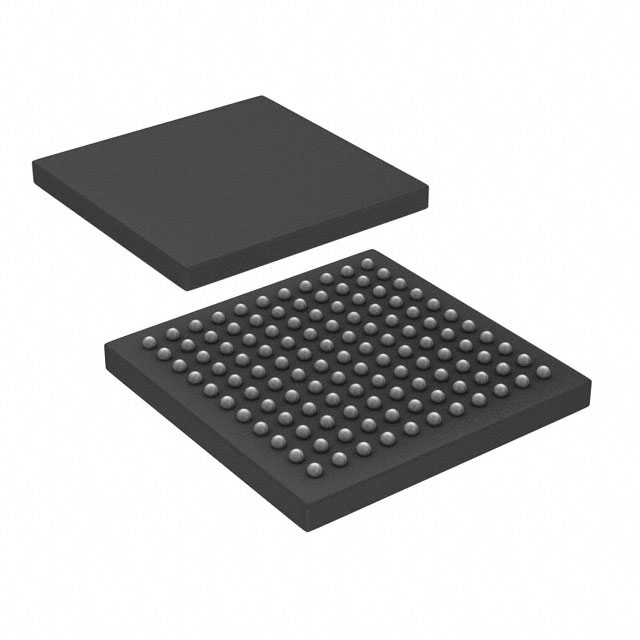
MCP37231-200I/TE
Active16-BIT, 200 MSPS, SINGLE PIPELINED ADC WITH 8-CHANNEL MUX 121 SIP 8X8X1.08MM TRAY ROHS COMPLIANT: YES
Deep-Dive with AI
Search across all available documentation for this part.

MCP37231-200I/TE
Active16-BIT, 200 MSPS, SINGLE PIPELINED ADC WITH 8-CHANNEL MUX 121 SIP 8X8X1.08MM TRAY ROHS COMPLIANT: YES
Deep-Dive with AI
Technical Specifications
Parameters and characteristics for this part
| Specification | MCP37231-200I/TE |
|---|---|
| Architecture | Pipelined |
| Configuration | MUX-ADC |
| Data Interface | LVDS - Parallel, Parallel |
| Input Type | Differential |
| Mounting Type | Surface Mount |
| Number of A/D Converters | 1 |
| Number of Bits | 16 |
| Number of Inputs | 8, 1, 2, 4 |
| Operating Temperature [Max] | 85 °C |
| Operating Temperature [Min] | -40 °C |
| Package / Case | 121-TFBGA |
| Reference Type | Internal |
| Sampling Rate (Per Second) | 200 M |
| Supplier Device Package | 121-TFBGA (8x8) |
| Voltage - Supply, Analog [Max] | 1.26 V, 1.89 V |
| Voltage - Supply, Analog [Min] | 1.71 V, 1.14 V |
| Voltage - Supply, Digital [Max] | 1.26 V, 1.89 V |
| Voltage - Supply, Digital [Min] | 1.14 V, 1.71 V |
Pricing
Prices provided here are for design reference only. For realtime values and availability, please visit the distributors directly
Description
General part information
MCP37231-200 Series
The MCP37231-200 is a 16-bit pipelined A/D converter with a maximum sampling rate of 200 Msps. The high accuracy of over 74 dB Signal-to-Noise Ratio (SNR) and over 90 dB Spurious Free Dynamic Range (SFDR) enable high precision measurements of fast input signals. The device operates at very low power consumption of 490 mW at 200 Msps including LVDS digital I/O. Lower power saving modes are available at 144 mW for Standby and 28 mW for Shutdown. The MCP37231-200 includes many digital processing features that simplify system design, cost and power usage. These include decimation filters for improved SNR, individual phase, offset and gain adjustment and a fractional delay recovery for time-delay corrections in multi-channel modes. Data is available through the serial DDR LVDS or parallel CMOS interface and configured via SPI. The device is available in the TFBGA-121 and VTLA-124 packages. TFBGA-121 package is qualified for automotive applications (AEC-Q100).
Documents
Technical documentation and resources


