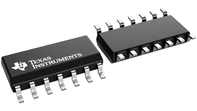
SN74LV74ADR
ActiveDUAL POSITIVE-EDGE-TRIGGERED D-TYPE FLIP-FLOPS
Deep-Dive with AI
Search across all available documentation for this part.

SN74LV74ADR
ActiveDUAL POSITIVE-EDGE-TRIGGERED D-TYPE FLIP-FLOPS
Technical Specifications
Parameters and characteristics for this part
| Specification | SN74LV74ADR |
|---|---|
| Clock Frequency | 140 MHz |
| Current - Output High, Low [custom] | 12 mA |
| Current - Output High, Low [custom] | 12 mA |
| Current - Quiescent (Iq) | 20 çA |
| Function | Reset, Set(Preset) |
| Input Capacitance | 2 pF |
| Max Propagation Delay @ V, Max CL | 9.3 ns |
| Mounting Type | Surface Mount |
| Number of Bits per Element | 1 |
| Number of Elements | 2 |
| Operating Temperature [Max] | 125 °C |
| Operating Temperature [Min] | -40 °C |
| Output Type | Complementary |
| Package / Case | 14-SOIC |
| Package / Case [x] | 0.154 in |
| Package / Case [y] | 3.9 mm |
| Trigger Type | Positive Edge |
| Type | D-Type |
| Voltage - Supply [Max] | 5.5 V |
| Voltage - Supply [Min] | 2 V |
Pricing
Prices provided here are for design reference only. For realtime values and availability, please visit the distributors directly
| Distributor | Package | Quantity | $ | |
|---|---|---|---|---|
| Digikey | Cut Tape (CT) | 1 | $ 0.41 | |
| 10 | $ 0.35 | |||
| 25 | $ 0.33 | |||
| 100 | $ 0.26 | |||
| 250 | $ 0.24 | |||
| 500 | $ 0.21 | |||
| 1000 | $ 0.16 | |||
| Digi-Reel® | 1 | $ 0.41 | ||
| 10 | $ 0.35 | |||
| 25 | $ 0.33 | |||
| 100 | $ 0.26 | |||
| 250 | $ 0.24 | |||
| 500 | $ 0.21 | |||
| 1000 | $ 0.16 | |||
| Tape & Reel (TR) | 2500 | $ 0.14 | ||
| 5000 | $ 0.14 | |||
| 12500 | $ 0.13 | |||
| 25000 | $ 0.12 | |||
| 62500 | $ 0.12 | |||
| Texas Instruments | LARGE T&R | 1 | $ 0.26 | |
| 100 | $ 0.18 | |||
| 250 | $ 0.14 | |||
| 1000 | $ 0.09 | |||
Description
General part information
SN74LV74A-Q1 Series
These dual positive-edge-triggered D-type flip-flops are designed for 2-V to 5.5-V VCCoperation.
A low level at the preset (PRE) or clear (CLR) inputs sets or resets the outputs, regardless of the levels of the other inputs. WhenPREandCLRare inactive (high), data at the data (D) inputs meeting the setup-time requirements is transferred to the outputs on the positive-going edge of the clock pulse. Clock triggering occurs at a voltage level and is not directly related to the rise time of the clock pulse. Following the hold-time interval, data at the D input can be changed without affecting the levels at the outputs.
This device is fully specified for partial-power-down applications using Ioff. The Ioffcircuitry disables the outputs, preventing damaging current backflow through the devices when they are powered down.
Documents
Technical documentation and resources


