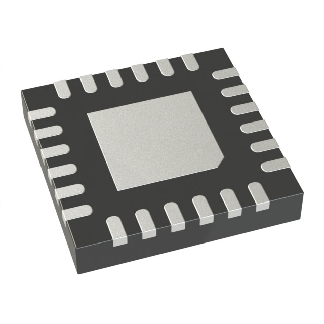
ADN2913ACPZ
ObsoleteCONTINUOUS RATE 6.5 MBPS TO 8.5 GBPS CLOCK AND DATA RECOVERY IC WITH INTEGRATED LIMITING AMP/EQ
Deep-Dive with AI
Search across all available documentation for this part.

ADN2913ACPZ
ObsoleteCONTINUOUS RATE 6.5 MBPS TO 8.5 GBPS CLOCK AND DATA RECOVERY IC WITH INTEGRATED LIMITING AMP/EQ
Technical Specifications
Parameters and characteristics for this part
| Specification | ADN2913ACPZ |
|---|---|
| Differential - Input:Output [custom] | True |
| Differential - Input:Output [custom] | True |
| Frequency - Max [Max] | 8.5 Gbps |
| Input | CML |
| Main Purpose | SONET/SDH |
| Mounting Type | Surface Mount |
| Number of Circuits | 1 |
| Operating Temperature [Max] | 85 °C |
| Operating Temperature [Min] | -40 °C |
| Output | CML |
| Package / Case | 24-WFQFN Exposed Pad, CSP |
| PLL | True |
| Ratio - Input:Output [custom] | 1:2 |
| Supplier Device Package | 24-LFCSP (4x4) |
| Voltage - Supply [Max] | 3.63 V |
| Voltage - Supply [Min] | 1.14 V |
Pricing
Prices provided here are for design reference only. For realtime values and availability, please visit the distributors directly
| Distributor | Package | Quantity | $ | |
|---|---|---|---|---|
Description
General part information
ADN2913 Series
The ADN2913 provides the receiver functions of quantization, signal level detection, and clock and data recovery for continuous data rates from 6.5 Mbps to 8.5 Gbps. The ADN2913 automatically locks to all data rates without the need for an external reference clock or programming. ADN2913 jitter performance exceeds all jitter specifications required by SONET/SDH, including jitter transfer, jitter generation, and jitter tolerance.The ADN2913 provides manual or automatic slice adjust and manual sample phase adjusts. Additionally, the user can select a limiting amplifier, equalizer, or 0 dB EQ at the input. The equalizer is adaptive or it can be manually set.The receiver front-end loss of signal (LOS) detector circuit indicates when the input signal level falls below a user-programmable threshold. The LOS detection circuit has hysteresis to prevent chatter at the LOS output. In addition, the input signal strength can be read through the I2C registers.The ADN2913 also supports pseudorandom binary sequence (PRBS) generation, bit error detection, and input data rate readback features.The ADN2913 is available in a compact 4 mm × 4 mm, 24-lead lead frame chip scale package (LFCSP). All ADN2913 specifications are defined over the ambient temperature range of −40°C to +85°C, unless otherwise noted.ApplicationsSONET/SDH OC-1/OC-3/OC-12/OC-48 and all associated FEC rates1GE, 1GFC, 2GFC, 4GFC, 8GFC, CPRI OS/L.6 up to OS/L.60Any rate regenerators/repeaters


