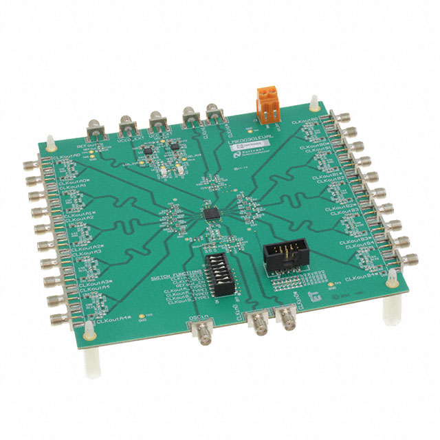
LMK00301EVAL/NOPB
ActiveLMK00301 CLOCK BUFFER AND DRIVER EVALUATION BOARD
Deep-Dive with AI
Search across all available documentation for this part.

LMK00301EVAL/NOPB
ActiveLMK00301 CLOCK BUFFER AND DRIVER EVALUATION BOARD
Deep-Dive with AI
Technical Specifications
Parameters and characteristics for this part
| Specification | LMK00301EVAL/NOPB |
|---|---|
| Contents | Board(s) |
| Embedded | False |
| Function | Clock Distribution |
| Supplied Contents | Board(s) |
| Type | Timing |
| Utilized IC / Part | LMK00301 |
Pricing
Prices provided here are for design reference only. For realtime values and availability, please visit the distributors directly
| Distributor | Package | Quantity | $ | |
|---|---|---|---|---|
| Digikey | Box | 1 | $ 358.80 | |
Description
General part information
LMK00301 Series
The LMK00301 is a 3-GHz, 10-output differential fanout buffer intended for high-frequency, low-jitter clock and data distribution, and level translation. The input clock can be selected from two universal inputs or one crystal input. The selected input clock is distributed to two banks of five differential outputs and one LVCMOS output. Both differential output banks can be independently configured as LVPECL, LVDS, or HCSL drivers, or disabled. The LVCMOS output has a synchronous enable input for runt-pulse-free operation when enabled or disabled. The LMK00301 operates from a 3.3-V core supply and three independent 3.3-V or 2.5-V output supplies.
The LMK00301 provides high performance, versatility, and power efficiency, making it ideal for replacing fixed-output buffer devices while increasing timing margin in the system. The LMK00301 offers a design spin, the LMK00301A, that does not have power supply sequencing requirements between the core and output supply domains.
The LMK00301 is a 3-GHz, 10-output differential fanout buffer intended for high-frequency, low-jitter clock and data distribution, and level translation. The input clock can be selected from two universal inputs or one crystal input. The selected input clock is distributed to two banks of five differential outputs and one LVCMOS output. Both differential output banks can be independently configured as LVPECL, LVDS, or HCSL drivers, or disabled. The LVCMOS output has a synchronous enable input for runt-pulse-free operation when enabled or disabled. The LMK00301 operates from a 3.3-V core supply and three independent 3.3-V or 2.5-V output supplies.
Documents
Technical documentation and resources


