LMK00301 Series
3-GHz, 10-output differential fanout buffer / level translator
Manufacturer: Texas Instruments
Catalog
3-GHz, 10-output differential fanout buffer / level translator
Key Features
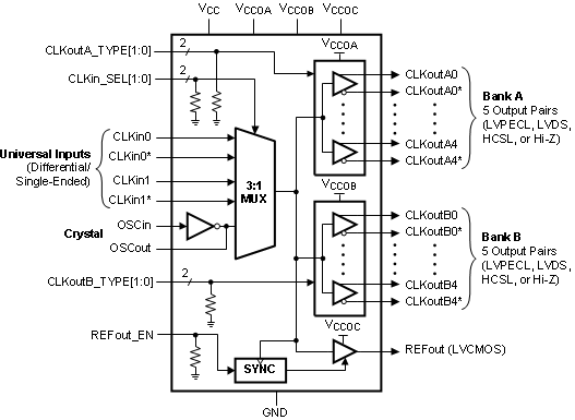
• 3:1 input multiplexerTwo universal inputs operate up to 3.1 ghz and accept lvpecl, lvds, cml, sstl, hstl, hcsl, or single-ended clocksOne crystal input accepts 10-mhz to 40-mhz crystal or single-ended clockTwo banks with five differential outputs eachLVPECL, LVDS, HCSL, or Hi-Z (selectable per bank)LVPECL additive jitter with lmk03806 clock source at 156.25 MHz:20 fs RMS (10 kHz to 1 MHz)51 fs RMS (12 kHz to 20 MHz)Frequency range:LVPECL (DC to 3100 MHz)LVDS (DC to 2100 MHz)HCSL (DC to 800 MHz)LVCMOS (DC to 250 MHz)High PSRR: –65 dBc (LVPECL) and –76 dBc (LVDS) at 156.25 MHzLVCMOS output with synchronous enable inputPin-controlled configurationV CC core supply: 3.3 V ± 5%Three independent V CCO output supplies: 3.3 V or 2.5 V ± 5%Industrial temperature range: –40°C to +85°C3:1 input multiplexerTwo universal inputs operate up to 3.1 ghz and accept lvpecl, lvds, cml, sstl, hstl, hcsl, or single-ended clocksOne crystal input accepts 10-mhz to 40-mhz crystal or single-ended clockTwo banks with five differential outputs eachLVPECL, LVDS, HCSL, or Hi-Z (selectable per bank)LVPECL additive jitter with lmk03806 clock source at 156.25 MHz:20 fs RMS (10 kHz to 1 MHz)51 fs RMS (12 kHz to 20 MHz)Frequency range:LVPECL (DC to 3100 MHz)LVDS (DC to 2100 MHz)HCSL (DC to 800 MHz)LVCMOS (DC to 250 MHz)High PSRR: –65 dBc (LVPECL) and –76 dBc (LVDS) at 156.25 MHzLVCMOS output with synchronous enable inputPin-controlled configurationV CC core supply: 3.3 V ± 5%Three independent V CCO output supplies: 3.3 V or 2.5 V ± 5%Industrial temperature range: –40°C to +85°C
Description
AI
The LMK00301 is a 3-GHz, 10-output differential fanout buffer intended for high-frequency, low-jitter clock and data distribution, and level translation. The input clock can be selected from two universal inputs or one crystal input. The selected input clock is distributed to two banks of five differential outputs and one LVCMOS output. Both differential output banks can be independently configured as LVPECL, LVDS, or HCSL drivers, or disabled. The LVCMOS output has a synchronous enable input for runt-pulse-free operation when enabled or disabled. The LMK00301 operates from a 3.3-V core supply and three independent 3.3-V or 2.5-V output supplies.
The LMK00301 provides high performance, versatility, and power efficiency, making it ideal for replacing fixed-output buffer devices while increasing timing margin in the system. The LMK00301 offers a design spin, the LMK00301A, that does not have power supply sequencing requirements between the core and output supply domains.


