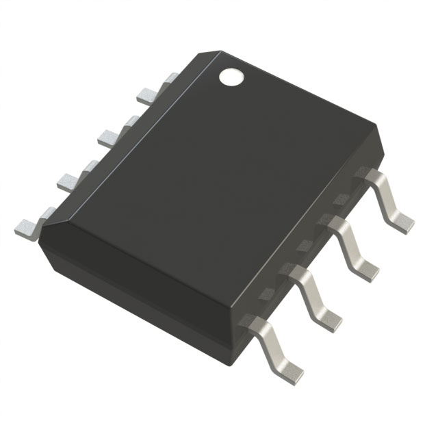
NLSX3012DR2G
Obsolete2-BIT 100 MBPS CONFIGURABLE DUAL-SUPPLY LEVEL TRANSLATOR

NLSX3012DR2G
Obsolete2-BIT 100 MBPS CONFIGURABLE DUAL-SUPPLY LEVEL TRANSLATOR
Technical Specifications
Parameters and characteristics for this part
| Specification | NLSX3012DR2G |
|---|---|
| Channel Type | Bidirectional |
| Channels per Circuit | 2 |
| Data Rate | 100 Mbps |
| Features | Auto-Direction Sensing |
| Mounting Type | Surface Mount |
| Number of Circuits | 1 |
| Operating Temperature [Max] | 85 °C |
| Operating Temperature [Min] | -40 °C |
| Output Type | Tri-State, Non-Inverted |
| Package / Case | 8-SOIC |
| Package / Case [x] | 0.154 in |
| Package / Case [y] | 3.9 mm |
| Supplier Device Package | 8-SOIC |
| Translator Type | Voltage Level |
| Voltage - VCCA [Max] | 4.5 V |
| Voltage - VCCA [Min] | 0.9 V |
| Voltage - VCCB [Max] | 4.5 V |
| Voltage - VCCB [Min] | 1.3 V |
Pricing
Prices provided here are for design reference only. For realtime values and availability, please visit the distributors directly
| Distributor | Package | Quantity | $ | |
|---|---|---|---|---|
| Newark | Each (Supplied on Full Reel) | 1 | $ 0.76 | |
| 3000 | $ 0.72 | |||
| 6000 | $ 0.66 | |||
| 12000 | $ 0.59 | |||
| 18000 | $ 0.57 | |||
| 30000 | $ 0.56 | |||
Description
General part information
NLSX3012 Series
The NLSX3012 is a 2 bit configurable dual-supply bidirectional level translator without a direction control pin. The I/O Vcc minus and I/O VL minus ports are designed to track two different power supply rails, Vcc and VL respectively. The VCC supply rail is configurable from 1.3 V to 4.5 V while the VL supply rail is configurable from 0.9 V to VCC minus 0.4V. This allows lower voltage logic signals on the VL side to be translated into higher voltage logic signals on the VCC side, and higher voltage logic signals on the VL side to be translated into lower voltage logic signals on the Vcc side. Both I/O ports are auto sensing; requiring no direction pin. The Output Enable input, when Low, disables both I/O ports by putting them in 3 state. This significantly reduces the supply currents from both Vcc and VL. The EN signal is designed to track VL.
Documents
Technical documentation and resources


