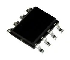
TDE1707BFP
ActivePOWER SWITCH HI SIDE/LO SIDE 0.5A 8-PIN SO N TUBE
Deep-Dive with AI
Search across all available documentation for this part.

TDE1707BFP
ActivePOWER SWITCH HI SIDE/LO SIDE 0.5A 8-PIN SO N TUBE
Deep-Dive with AI
Technical Specifications
Parameters and characteristics for this part
| Specification | TDE1707BFP |
|---|---|
| Current - Output (Max) [Max] | 500 mA |
| Fault Protection | Current Limiting (Fixed), Over Temperature |
| Features | 5V Regulated Output |
| Input Type | Non-Inverting |
| Interface | On/Off |
| Mounting Type | Surface Mount |
| Number of Outputs | 2 |
| Operating Temperature [Max] | 85 °C |
| Operating Temperature [Min] | -25 °C |
| Output Configuration | High Side or Low Side |
| Output Type | Bipolar |
| Package / Case | 0.154 in |
| Package / Case | 8-SOIC |
| Package / Case | 3.9 mm |
| Ratio - Input:Output | 1:2 |
| Supplier Device Package | 8-SOIC |
| Switch Type | General Purpose |
| Voltage - Load [Max] | 48 V |
| Voltage - Load [Min] | 6 V |
| Voltage - Supply (Vcc/Vdd) | Not Required |
Pricing
Prices provided here are for design reference only. For realtime values and availability, please visit the distributors directly
Description
General part information
TDE1707 Series
The TDE1707BFP and TDE1707CFP are 0.5 A integrated power switches with up to 48 V power supply capability. Two output configurations are possible. The former is the load to GND (high-side mode) and the latter is the load to VS(low-side mode). This device is dedicated to proximity detectors; its internal +5 V supply can be used to supply external circuits (please refer to AN495 and AN1213 on www.st.com). A signal is internally generated to block the IN signal, and prevent the output switch, as long as an abnormal condition is detected. The power-on transition, as well as the chip overtemperature and the output overcurrent, generate this signal. A minimum delay of 25 μs (typ. value) is added to the trailing edge of this signal to ensure that a stable normal situation is present when the signal disappears. The delay (the disappearance of block signal) can be further increased by connecting a capacitor between pin 3 and ground. It can drive resistive or inductive loads.
Documents
Technical documentation and resources


