Deep-Dive with AI
Search across all available documentation for this part.

Deep-Dive with AI
Technical Specifications
Parameters and characteristics for this part
| Specification | DAC312ER |
|---|---|
| Architecture | R-2R |
| Data Interface | Parallel |
| Differential Output | True |
| INL/DNL (LSB) | ±0.5 (Max), - |
| Mounting Type | Through Hole |
| Number of Bits | 12 bits |
| Operating Temperature [Max] | 70 °C |
| Operating Temperature [Min] | 0 °C |
| Output Type | Current - Unbuffered |
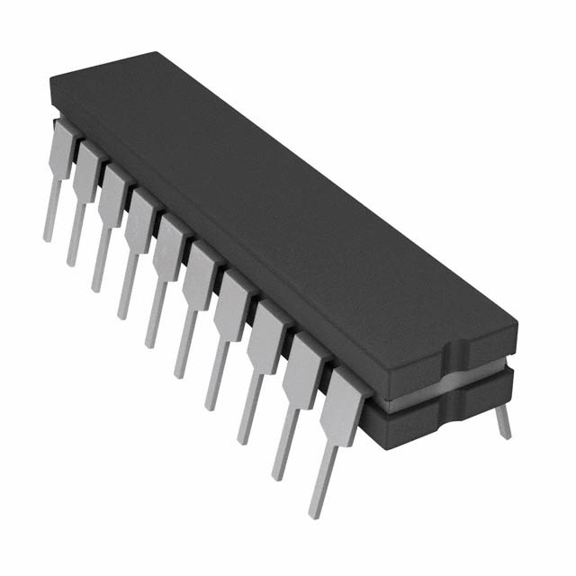
| Package / Case | 20-CDIP |
| Reference Type | External |
| Settling Time | 500 ns |
| Supplier Device Package | 20-CERDIP |
| Voltage - Supply, Analog [Max] | 18 V |
| Voltage - Supply, Analog [Min] | -10.8 V, 4.5 V |
| Voltage - Supply, Digital [Max] | 36 V |
| Voltage - Supply, Digital [Min] | 20 V |
Pricing
Prices provided here are for design reference only. For realtime values and availability, please visit the distributors directly
| Distributor | Package | Quantity | $ | |
|---|---|---|---|---|
| Digikey | Tube | 18 | $ 67.38 | |
Description
General part information
DAC312 Series
The DAC312 series of 12-bit multiplying digital-to-analog converters provide high speed with guaranteed performance to 0.012% differential nonlinearity over the full commercial operating temperature range.The DAC312 combines a 9-bit master D/A converter with a 3-bit (MSBs) segment generator to form an accurate 12-bit D/A converter at low cost. This technique guarantees a very uniform step size (up to ±1/2 LSB from the ideal), monotonicity to 12-bits and integral nonlinearity to 0.05% at its differential current outputs. In order to provide the same performance with a 12-bit R-2R ladder design, an integral nonlinearity over temperature of 1/2 LSB (0.012%) would be required.The 250 ns settling time with low glitch energy and low power consumption are achieved by careful attention to the circuit design and stringent process controls. Direct interface with all popular logic families is achieved through the logic threshold terminal.High compliance and low drift characteristics (as low as 10 ppm/°C) are also features of the DAC312 along with an excellent power supply rejection ratio of ±.001% FS/%∆V. Operating over a power supply range of +5/–11 V to ±18 V the device consumes 225 mW at the lower supply voltages with an absolute maximum dissipation of 375 mW at the higher supply levels.With their guaranteed specifications, single chip reliability and low cost, the DAC312 device makes excellent building blocks for A/D converters, data acquisition systems, video display drivers, programmable test equipment and other applications where low power consumption and complete input/output versatility are required.
Documents
Technical documentation and resources


