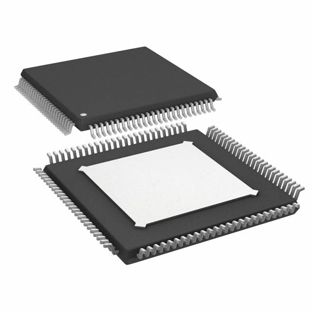
AD9277BSVZ
ActiveAFE GENERAL PURPOSE 1 ADC 14BIT 100-PIN TQFP EP TRAY
Deep-Dive with AI
Search across all available documentation for this part.

AD9277BSVZ
ActiveAFE GENERAL PURPOSE 1 ADC 14BIT 100-PIN TQFP EP TRAY
Technical Specifications
Parameters and characteristics for this part
| Specification | AD9277BSVZ |
|---|---|
| Data Interface | SPI |
| Mounting Type | Surface Mount |
| Number of Channels | 8 |
| Operating Temperature [Max] | 85 °C |
| Operating Temperature [Min] | -40 °C |
| Package / Case | 100-TQFP Exposed Pad |
| Resolution (Bits) | 14 b |
| Sampling Rate (Per Second) [Max] | 50 M |
| Sampling Rate (Per Second) [Min] | 10 M |
| Type | AAF, Demodulator, LNA, VGA, ADC |
| Voltage - Supply | 3 V, 1.8 V |
| Voltage Supply Source | Analog and Digital |
Pricing
Prices provided here are for design reference only. For realtime values and availability, please visit the distributors directly
Description
General part information
AD9277 Series
The AD9277 is designed for low cost, low power, small size, and ease of use. It contains eight channels of a variable gain amplifier (VGA) with a low noise preamplifier (LNA); an anti-aliasing filter (AAF); a 14-bit, 10 MSPS to 50 MSPS analog-to-digital converter (ADC); and an I/Q demodulator with programmable phase rotation.Each channel features a variable gain range of 42 dB, a fully differ-ential signal path, an active input preamplifier termination, a maximum gain of up to 52 dB, and an ADC with a conversion rate of up to 50 MSPS. The channel is optimized for dynamic performance and low power in applications where a small package size is critical.The LNA has a single-ended-to-differential gain that is selectable through the SPI. The LNA input noise is typically 0.75 nV/√Hz at a gain of 21.3 dB, and the combined input-referred noise of the entire channel is 0.85 nV/√Hz at maximum gain. Assuming a 15 MHz noise bandwidth (NBW) and a 21.3 dB LNA gain, the input SNR is roughly 92 dB. In CW Doppler mode, each LNA output drives an I/Q demodulator. Each demodulator has inde-pendently programmable phase rotation through the SPI with 16 phase settings.The AD9277 requires a LVPECL-/CMOS-/LVDS-compatible sample rate clock for full performance operation. No external reference or driver components are required for many applications.The ADC automatically multiplies the sample rate clock for the appropriate LVDS serial data rate. A data clock (DCO±) for capturing data on the output and a frame clock (FCO±) trigger for signaling a new output byte are provided.Powering down individual channels is supported to increase battery life for portable applications. A standby mode option allows quick power-up for power cycling. In CW Doppler opera-tion, the VGA, AAF, and ADC are powered down. The power of the TGC path scales with selectable ADC speed power modes.The ADC contains several features designed to maximize flexibility and minimize system cost, such as a programmable clock, data alignment, and programmable digital test pattern generation. The digital test patterns include built-in fixed patterns, built-in pseudo-random patterns, and custom user-defined test patterns entered via the serial port interface.Fabricated in an advanced CMOS process, the AD9277 is available in a 16 mm × 16 mm, RoHS compliant, 100-lead TQFP. It is specified over the industrial temperature range of −40°C to +85°C.ApplicationsMedical imaging/ultrasoundAutomotive radar


