Deep-Dive with AI
Search across all available documentation for this part.

Deep-Dive with AI
Technical Specifications
Parameters and characteristics for this part
| Specification | AD5622ACPZ-2-RL7 |
|---|---|
| Architecture | String DAC |
| Data Interface | I2C |
| Differential Output | False |
| INL/DNL (LSB) | 1 LSB |
| INL/DNL (LSB) | 6 LSB |
| Mounting Type | Surface Mount |
| Number of Bits | 12 bits |
| Operating Temperature [Max] | 125 °C |
| Operating Temperature [Min] | -40 °C |
| Output Type | Voltage - Buffered |
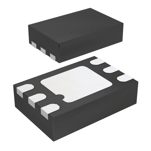
| Package / Case | 6-VDFN Exposed Pad, CSP |
| Reference Type | Supply |
| Settling Time | 10 µs |
| Supplier Device Package | 6-LFCSP-WD (2x3) |
| Voltage - Supply, Analog [Max] | 5.5 V |
| Voltage - Supply, Analog [Min] | 2.7 V |
| Voltage - Supply, Digital [Max] | 5.5 V |
| Voltage - Supply, Digital [Min] | 2.7 V |
Pricing
Prices provided here are for design reference only. For realtime values and availability, please visit the distributors directly
| Distributor | Package | Quantity | $ | |
|---|---|---|---|---|
Description
General part information
AD5622 Series
TheAD5602/AD5612/ AD5622, members of thenanoDAC®family, are single 8-/10-/12-bit buffered voltage-out DACs that operates from a single 2.7 V to 5.5 V supply, consuming <100 µA at 5 V. The AD5602 / AD5612 / AD5622 comes in a tiny LFCSP and SC70 packages. Each DAC contains an on-chip precision output amplifier allows rail-to-rail output swing to be achieved.The AD5602 / AD5612 / AD5622 utilizes a 2-wire I2C-compatible serial interface that operates in standard (100 KHz), fast (400 KHz) and high speed (3.4 MHz) modes.The references for AD5602 / AD5612 / AD5622 are derived from the power supply inputs and to give the widest dynamic output range. Each part incorporates a power-on reset circuit that ensures the DAC output powers up to 0 V and remains there until a valid write takes place to the device. The part contains a power-down feature that reduces the current consumption of the device to <150 nA at 3 V and provides software selectable output loads while in power-down mode. The devices are put into power-down mode over the serial interface. The low power consumption of the AD5602 / AD5612 / AD5622 in normal operation makes them ideally suited to portable battery operated equipment. The power consumption is 0.4 mW at 5 V.PRODUCT HIGHLIGHTSAvailable in 6-lead LFCSP and SC70 packages.Max 100µA power consumption, single-supply operation. This part operates from a single 2.7 V to 5.5 V supply and typically consumes 0.2 mW at 3 V and 0.4 mW at 5 V, making it ideal for battery-powered applications.The on-chip output buffer amplifier allows the output of the DAC to swing rail-to-rail with a typical slew rate of 0.5 V/µs.Reference derived from the power supply.Standard, fast and high speed mode I2C interface.Designed for very low power consumption.Power-down capability. When powered down, the DAC typically consumes <150 nA at 3 V.Power-on-reset and brown out detection.APPLICATIONSProcess controlData acquisition systemsPortable battery-powered instrumentsDigital gain and offset adjustmentProgrammable voltage and current sourcesProgrammable attenuators
Documents
Technical documentation and resources


