Deep-Dive with AI
Search across all available documentation for this part.

Deep-Dive with AI
Technical Specifications
Parameters and characteristics for this part
| Specification | AD7490BRU |
|---|---|
| Architecture | SAR |
| Configuration | MUX-S/H-ADC |
| Data Interface | DSP, SPI |
| Input Type | Single Ended |
| Mounting Type | Surface Mount |
| Number of A/D Converters | 1 |
| Number of Bits | 12 bits |
| Number of Inputs | 16 |
| Operating Temperature [Max] | 85 °C |
| Operating Temperature [Min] | -40 °C |
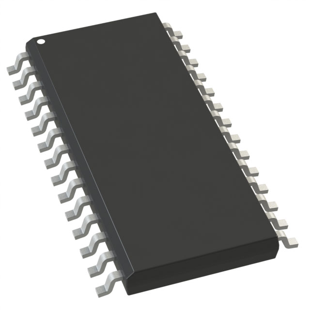
| Package / Case | 28-TSSOP |
| Package / Case | 0.173 in |
| Package / Case [y] | 4.4 mm |
| Ratio - S/H:ADC | 1:1 |
| Reference Type | External |
| Sampling Rate (Per Second) | 1 M |
| Supplier Device Package | 28-TSSOP |
| Voltage - Supply, Analog [Max] | 5.25 V |
| Voltage - Supply, Analog [Min] | 2.7 V |
| Voltage - Supply, Digital [Max] | 5.25 V |
| Voltage - Supply, Digital [Min] | 2.7 V |
Pricing
Prices provided here are for design reference only. For realtime values and availability, please visit the distributors directly
| Distributor | Package | Quantity | $ | |
|---|---|---|---|---|
Description
General part information
AD7490 Series
The AD7490 is a 12-bit high speed, low power, 16-channel, successive approximation ADC. The part operates from a single 2.7 V to 5.25 V power supply and features throughput rates up to 1 MSPS. The part contains a low noise, wide bandwidth track-and-hold amplifier that can handle input frequencies in excess of 1 MHz.The conversion process and data acquisition are controlled usingCSand the serial clock signal, allowing the device to easily interface with microprocessors or DSPs. The input signal is sampled on the falling edge ofCS, and conversion is also initiated at this point. There are no pipeline delays associated with the part.The AD7490 uses advanced design techniques to achieve very low power dissipation at high throughput rates. For maximum throughput rates, the AD7490 consumes just 1.8 mA with 3 V supplies, and 2.5 mA with 5 V supplies.By setting the relevant bits in the control register, the analog input range for the part can be selected to be a 0 V to REFIN input or a 0 V to 2 × REFIN input, with either straight binary or twos complement output coding. The AD7490 features 16 single-ended analog inputs with a channel sequencer to allow a preprogrammed selection of channels to be converted sequen-tially. The conversion time is determined by the SCLK frequency because this is also used as the master clock to control the conversion.The AD7490 is available in a 32-lead LFCSP and a 28-lead TSSOP package.APPLICATIONSMultichannel system monitoringBattery-powered equipmentPower line monitoringData acquisition, instrumentation, and process control
Documents
Technical documentation and resources


