CLV8T595QWBQBRQ1
ActiveAUTOMOTIVE EIGHT-BIT SHIFT REGISTER WITH TRI-STATE OUTPUT REGISTERS AND LOGIC-LEVEL SHIFTER
Deep-Dive with AI
Search across all available documentation for this part.

CLV8T595QWBQBRQ1
ActiveAUTOMOTIVE EIGHT-BIT SHIFT REGISTER WITH TRI-STATE OUTPUT REGISTERS AND LOGIC-LEVEL SHIFTER
Deep-Dive with AI
Technical Specifications
Parameters and characteristics for this part
| Specification | CLV8T595QWBQBRQ1 |
|---|---|
| Function | Serial to Parallel, Serial |
| Grade | Automotive |
| Logic Type | Shift Register |
| Mounting Type | Wettable Flank, Surface Mount |
| Number of Bits per Element | 8 |
| Number of Elements | 1 |
| Operating Temperature [Max] | 125 °C |
| Operating Temperature [Min] | -40 °C |
| Output Type | Push-Pull |
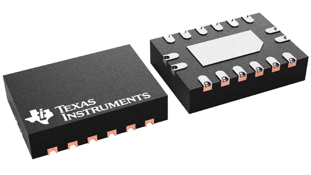
| Package / Case | 16-WFQFN Exposed Pad |
| Qualification | AEC-Q100 |
| Supplier Device Package | 16-WQFN (2.5x3.5) |
| Voltage - Supply [Max] | 5.5 V |
| Voltage - Supply [Min] | 1.65 V |
Pricing
Prices provided here are for design reference only. For realtime values and availability, please visit the distributors directly
| Distributor | Package | Quantity | $ | |
|---|---|---|---|---|
| Digikey | Tape & Reel (TR) | 3000 | $ 0.45 | |
| 6000 | $ 0.43 | |||
| 15000 | $ 0.41 | |||
| Texas Instruments | LARGE T&R | 1 | $ 0.79 | |
| 100 | $ 0.61 | |||
| 250 | $ 0.45 | |||
| 1000 | $ 0.32 | |||
Description
General part information
SN74LV8T595-Q1 Series
The SN74LV8T595-Q1 device contains an 8-bit, serial-in, parallel-out shift register that feeds an 8-bit D-type storage register. The storage register has parallel 3-state outputs. Separate clocks are provided for both the shift and storage register. The shift register has a direct overriding clear (SRCLR) input, serial (SER) input, and a serial output (QH’) for cascading. When the output-enable (OE) input is high, the storage register outputs are in a high-impedance state. Internal register data and serial output (QH’) are not impacted by the operation of the OE input.
The input is designed with a reduced threshold circuit to support up translation when the supply voltage is larger than the input voltage. Additionally, the 5V tolerant input pins enable down translation when the input voltage is larger than the supply voltage. The output level is always referenced to the supply voltage (VCC) and supports 1.8V, 2.5V, 3.3V, and 5V CMOS levels.
The SN74LV8T595-Q1 device contains an 8-bit, serial-in, parallel-out shift register that feeds an 8-bit D-type storage register. The storage register has parallel 3-state outputs. Separate clocks are provided for both the shift and storage register. The shift register has a direct overriding clear (SRCLR) input, serial (SER) input, and a serial output (QH’) for cascading. When the output-enable (OE) input is high, the storage register outputs are in a high-impedance state. Internal register data and serial output (QH’) are not impacted by the operation of the OE input.
Documents
Technical documentation and resources


