SN74LV8T595-Q1 Series
Automotive eight-bit shift register with tri-state output registers and logic-level shifter
Manufacturer: Texas Instruments
Catalog
Automotive eight-bit shift register with tri-state output registers and logic-level shifter
Key Features
• AEC-Q100 qualified for automotive applications:Device temperature grade 1: -40°C to +125°CDevice HBM ESD classification level 2Device CDM ESD classification level C4BAvailable in wettable flank QFN packageLatching logic with known power-up state provides consistent start-up behaviorWide operating range of 1.65V to 5.5V5.5V tolerant input pinsSingle-supply voltage translator (refer to LVxT Enhanced Input Voltage):Up translation:1.2V to 1.8V1.5V to 2.5V1.8V to 3.3V3.3V to 5.0VDown translation:5.0V, 3.3V, 2.5V to 1.8V5.0V, 3.3V to 2.5V5.0V to 3.3VUp to 150Mbps with 5V or 3.3V VCCSupports standard function pinoutLatch-up performance exceeds 250mAper JESD 17AEC-Q100 qualified for automotive applications:Device temperature grade 1: -40°C to +125°CDevice HBM ESD classification level 2Device CDM ESD classification level C4BAvailable in wettable flank QFN packageLatching logic with known power-up state provides consistent start-up behaviorWide operating range of 1.65V to 5.5V5.5V tolerant input pinsSingle-supply voltage translator (refer to LVxT Enhanced Input Voltage):Up translation:1.2V to 1.8V1.5V to 2.5V1.8V to 3.3V3.3V to 5.0VDown translation:5.0V, 3.3V, 2.5V to 1.8V5.0V, 3.3V to 2.5V5.0V to 3.3VUp to 150Mbps with 5V or 3.3V VCCSupports standard function pinoutLatch-up performance exceeds 250mAper JESD 17
Description
AI
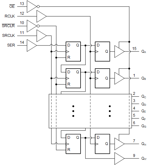
The SN74LV8T595-Q1 device contains an 8-bit, serial-in, parallel-out shift register that feeds an 8-bit D-type storage register. The storage register has parallel 3-state outputs. Separate clocks are provided for both the shift and storage register. The shift register has a direct overriding clear (SRCLR) input, serial (SER) input, and a serial output (QH’) for cascading. When the output-enable (OE) input is high, the storage register outputs are in a high-impedance state. Internal register data and serial output (QH’) are not impacted by the operation of the OE input.
The input is designed with a reduced threshold circuit to support up translation when the supply voltage is larger than the input voltage. Additionally, the 5V tolerant input pins enable down translation when the input voltage is larger than the supply voltage. The output level is always referenced to the supply voltage (VCC) and supports 1.8V, 2.5V, 3.3V, and 5V CMOS levels.


