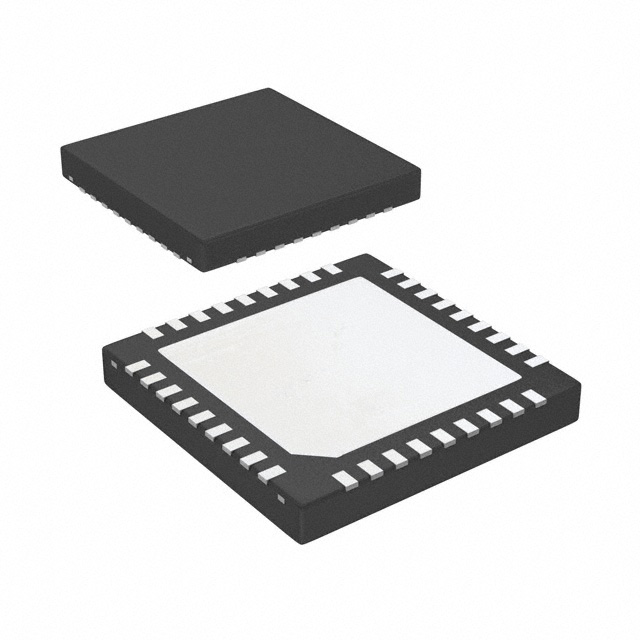
DS90UR907QSQ/NOPB
Active5 - 65 MHZ 24-BIT COLOR FPD-LINK TO FPD-LINK II CONVERTER
Deep-Dive with AI
Search across all available documentation for this part.

DS90UR907QSQ/NOPB
Active5 - 65 MHZ 24-BIT COLOR FPD-LINK TO FPD-LINK II CONVERTER
Technical Specifications
Parameters and characteristics for this part
| Specification | DS90UR907QSQ/NOPB |
|---|---|
| Data Rate | 1.82 Gbps |
| Function | Serializer |
| Grade | Automotive |
| Mounting Type | Surface Mount |
| Number of Inputs | 5 |
| Number of Outputs | 1 |
| Operating Temperature [Max] | 105 °C |
| Operating Temperature [Min] | -40 °C |
| Output Type | FPD-Link II, LVDS |
| Package / Case | 36-WFQFN Exposed Pad |
| Qualification | AEC-Q100 |
| Supplier Device Package | 36-WQFN (6x6) |
| Voltage - Supply [Max] | 3.6 V, 1.89 V |
| Voltage - Supply [Min] | 3 V, 1.71 V |
Pricing
Prices provided here are for design reference only. For realtime values and availability, please visit the distributors directly
| Distributor | Package | Quantity | $ | |
|---|---|---|---|---|
| Digikey | Cut Tape (CT) | 1 | $ 17.24 | |
| Digi-Reel® | 1 | $ 17.24 | ||
| Tape & Reel (TR) | 1000 | $ 8.67 | ||
| Texas Instruments | SMALL T&R | 1 | $ 11.51 | |
| 100 | $ 10.06 | |||
| 250 | $ 7.75 | |||
| 1000 | $ 6.93 | |||
Description
General part information
DS90UR907Q-Q1 Series
The DS90UR907Q-Q1 converts FPD-Link to FPD-Link II. It translates four LVDS data/control streams and one LVDS clock pair (FPD-Link) into a high-speed serialized interface (FPD-Link II) over a single pair. This serial bus scheme greatly eases system design by eliminating skew problems between clock and data, reduces the number of connector pins, reduces the interconnect size, weight, and cost, and overall eases PCB layout. In addition, internal DC balanced encoding is used to support AC-coupled interconnects.
The DS90UR907Q-Q1 converts, balances and level shifts four LVDS data/control streams, and embeds one LVDS clock pair (FPD-Link) to a serial stream (FPD-Link II). Up to 24 bits of RGB in the FPD-Link are serialized along with the three video control signals.
Serial transmission is optimized by a user selectable de-emphasis and differential output level select features. EMI is minimized by the use of low voltage differential signaling and spread spectrum clocking compatibility.
Documents
Technical documentation and resources


