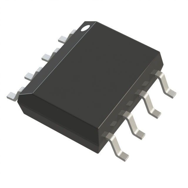
AD8207WBRZ-RL
ActiveZERO DRIFT, HIGH VOLTAGE, BIDIRECTIONAL DIFFERENCE AMPLIFIER
Deep-Dive with AI
Search across all available documentation for this part.

AD8207WBRZ-RL
ActiveZERO DRIFT, HIGH VOLTAGE, BIDIRECTIONAL DIFFERENCE AMPLIFIER
Deep-Dive with AI
Technical Specifications
Parameters and characteristics for this part
| Specification | AD8207WBRZ-RL |
|---|---|
| -3db Bandwidth | 150 kHz |
| Amplifier Type | Zero-Drift |
| Current - Supply | 2.5 mA |
| Grade | Automotive |
| Mounting Type | Surface Mount |
| Number of Circuits | 1 |
| Operating Temperature [Max] | 125 °C |
| Operating Temperature [Min] | -40 °C |
| Package / Case | 8-SOIC |
| Package / Case [x] | 0.154 in |
| Package / Case [y] | 3.9 mm |
| Slew Rate | 1 V/µs |
| Supplier Device Package | 8-SOIC |
| Voltage - Input Offset | 100 çV |
| Voltage - Supply Span (Max) [Max] | 5.5 V |
| Voltage - Supply Span (Min) [Min] | 3.3 V |
Pricing
Prices provided here are for design reference only. For realtime values and availability, please visit the distributors directly
| Distributor | Package | Quantity | $ | |
|---|---|---|---|---|
| Digikey | Cut Tape (CT) | 1 | $ 6.23 | |
| 10 | $ 4.30 | |||
| 25 | $ 3.80 | |||
| 100 | $ 3.67 | |||
| Digi-Reel® | 1 | $ 6.23 | ||
| 10 | $ 4.30 | |||
| 25 | $ 3.80 | |||
| 100 | $ 3.67 | |||
| Tape & Reel (TR) | 2500 | $ 3.67 | ||
Description
General part information
AD8207 Series
The AD8207 is a single-supply difference amplifier ideal for amplifying small differential voltages in the presence of large common-mode voltage. The operating input common-mode voltage range extends from −4 V to +65 V with a 5 V supply. The AD8207 works with a single-supply voltage of 3.3 V to 5 V, and is ideally suited to withstand large input PWM common-mode voltages, typical in solenoid and motor control applications.The AD8207 is available in an 8-lead SOIC package. Excellent dc performance over temperature keeps errors in the mea-surement loop to a minimum. Offset drift is typically less than 500 nV/°C, and gain drift is typically below 10 ppm/°C.The AD8207 is ideal for bidirectional current sensing applications. It features two reference pins,VREF1 and VREF2, that allow the user to easily offset the output of the device to any voltage within the supply range. With VREF1 attached to the V+ pin and VREF2 attached to the GND pin, the output is set at half scale. Attaching both pins to GND causes the output to be unipolar, starting near ground. Attaching both pins to V+ causes the output to be unipolar starting near V+. Other output offsets are achieved by applying an external low impedance voltage to the VREF1 and VREF2 pins.ApplicationsHigh-side current sensing inMotor controlSolenoid controlDiesel-injection controlEngine managementSuspension controlVehicle dynamic controlDC-to-dc converters
Documents
Technical documentation and resources


