Deep-Dive with AI
Search across all available documentation for this part.

Deep-Dive with AI
Technical Specifications
Parameters and characteristics for this part
| Specification | AD7247KN |
|---|---|
| Architecture | R-2R |
| Data Interface | Parallel |
| Differential Output | False |
| INL/DNL (LSB) | 0.5 LSB, 0.9 LSB |
| Mounting Type | Through Hole |
| Number of Bits | 12 bits |
| Operating Temperature [Max] | 85 °C |
| Operating Temperature [Min] | -40 °C |
| Output Type | Voltage - Buffered |
| Package / Case | 0.3 in |
| Package / Case | 24-DIP |
| Package / Case | 7.62 mm |
| Reference Type | External, Internal |
| Settling Time | 10 µs |
| Supplier Device Package | 24-PDIP |
| Voltage - Supply, Analog [Max] | 15 V |
| Voltage - Supply, Analog [Min] | -15 V |
| Voltage - Supply, Digital | 15 V |
Pricing
Prices provided here are for design reference only. For realtime values and availability, please visit the distributors directly
| Distributor | Package | Quantity | $ | |
|---|---|---|---|---|
Description
General part information
AD7247 Series
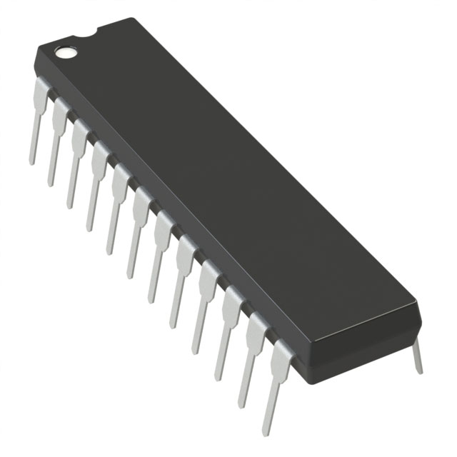
The AD7237A / AD7247A is an enhanced version of the industry standardAD7237/ AD7247. Improvements include operation from 12 V to 15 V supplies, faster interface times and better reference variations with VDD. Additional features include faster settling times.The AD7237A / AD7247A is a complete, dual, 12-bit, voltage output digital-to-analog converter with output amplifiers and Zener voltage reference on a monolithic CMOS chip. No external user trims are required to achieve full specified performance.Both parts are microprocessor compatible, with high speed data latches and interface logic. The AD7247A accepts 12-bit parallel data which is loaded into the respective DAC latch using theWRinput and a separate Chip Select input for each DAC. The AD7237A has a double buffered interface structure and an 8-bit wide data bus with data loaded to the respective input latch in two write operations. An asynchronousLDACsignal on the AD7237A updates the DAC latches and analog outputs.A REF OUT/REF IN function is provided which allows either the on-chip 5 V reference or an external reference to be used as a reference voltage for the part. For single supply operation, two output ranges of 0 V to +5 V and 0 V to +10 V are available, while these two ranges plus an additional ±5 V range are available with dual supplies. The output amplifiers are capable of developing +10 V across a 2 kΩ load to GND.The AD7237A / AD7247A is fabricated in Linear Compatible CMOS (LC2MOS), an advanced, mixed technology process that combines precision bipolar circuits with low power CMOS logic. Both parts are available in a 24-pin, 0.3" wide plastic and hermetic dual-in-line package (DIP) and are also packaged in a 24-lead small outline (SOIC) package.
Documents
Technical documentation and resources


