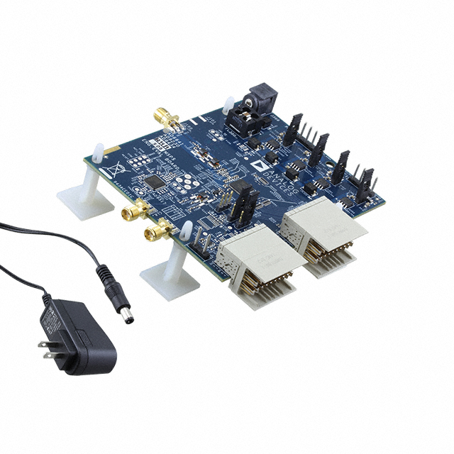

Technical Specifications
Parameters and characteristics for this part
| Specification | AD9484-500EBZ |
|---|---|
| Contents | Board(s) |
| Data Interface | SPI |
| Input Range | 1.5 Vpp |
| Number of A/D Converters | 1 |
| Number of Bits | 8 |
| Power (Typ) @ Conditions | 670 mW |
| Sampling Rate (Per Second) | 500 M |
| Utilized IC / Part | AD9484 |
Pricing
Prices provided here are for design reference only. For realtime values and availability, please visit the distributors directly
| Distributor | Package | Quantity | $ | |
|---|---|---|---|---|
| Digikey | Box | 1 | $ 312.34 | |
Description
General part information
AD9484 Series
The AD9484 is an 8-bit, monolithic, sampling analog-to-digital converter (ADC) optimized for high performance, low power, and ease of use. The part operates at up to a 500 MSPS conversion rate and is optimized for outstanding dynamic performance in wideband carrier and broadband systems. All necessary functions, including a sample-and-hold and voltage reference, are included on the chip to provide a complete signal conversion solution. The VREF pin can be used to monitor the internal reference or provide an external voltage reference (external reference mode must be enabled through the SPI port).The ADC requires a 1.8 V analog voltage supply and a differential clock for full performance operation. The digital outputs are LVDS (ANSI-644) compatible and support twos complement, offset binary format, or Gray code. A data clock output is available for proper output data timing.Fabricated on an advanced BiCMOS process, the AD9484 is available in a 56-lead LFCSP, and is specified over the industrial temperature range (−40°C to +85°C). This product is protected under U.S. and international patents.PRODUCT HIGHLIGHTSHigh Performance.Maintains 47 dBFS SNR at 500 MSPS with a 250 MHz input.Ease of Use.LVDS output data and output clock signal allow interface to current FPGA technology. The on-chip reference and sample and hold provide flexibility in system design. Use of a single 1.8 V supply simplifies system power supply design.Serial Port Control.Standard serial port interface supports various product functions, such as data formatting, disabling the clock duty cycle stabilizer, power down, gain adjust, and output test pattern generation.APPLICATIONSWireless and wired broadband communicationsCable reverse pathCommunications test equipmentLow cost digital oscilloscopesSatellite subsystemsPower amplifier linearization
Documents
Technical documentation and resources


