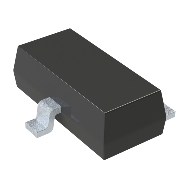
NDS356AP-NB8L005A
Obsolete-30V P-CHANNEL LOGIC LEVEL ENHANCEMENT MODE FIELD EFFECT TRANSISTOR
Deep-Dive with AI
Search across all available documentation for this part.

NDS356AP-NB8L005A
Obsolete-30V P-CHANNEL LOGIC LEVEL ENHANCEMENT MODE FIELD EFFECT TRANSISTOR
Deep-Dive with AI
Technical Specifications
Parameters and characteristics for this part
| Specification | NDS356AP-NB8L005A |
|---|---|
| Current - Continuous Drain (Id) @ 25°C | 1.1 A |
| Drain to Source Voltage (Vdss) | 30 V |
| Drive Voltage (Max Rds On, Min Rds On) | 10 V, 4.5 V |
| FET Type | P-Channel |
| Input Capacitance (Ciss) (Max) @ Vds | 280 pF |
| Mounting Type | Surface Mount |
| Operating Temperature [Max] | 150 °C |
| Operating Temperature [Min] | -55 °C |
| Package / Case | SOT-23-3, TO-236-3, SC-59 |
| Power Dissipation (Max) [Max] | 500 mW |
| Rds On (Max) @ Id, Vgs [Max] | 200 mOhm |
| Supplier Device Package | SOT-23-3 |
| Technology | MOSFET (Metal Oxide) |
| Vgs (Max) | 20 V |
| Vgs(th) (Max) @ Id | 2.5 V |
Pricing
Prices provided here are for design reference only. For realtime values and availability, please visit the distributors directly
| Distributor | Package | Quantity | $ | |
|---|---|---|---|---|
Description
General part information
NDS356AP Series
SuperSOT™-3 P-Channel logic level enhancement mode power field effect transistors are produced using ON Semiconductor's proprietary, high cell density, DMOS technology. This very high density process is especially tailored to minimize on-state resistance. These devices are particularly suited for low voltage applications such as notebook computer power management, portable electronics, and other battery powered circuits where fast high-side switching, and low in-line power loss are needed in a very small outline surface mount package.
Documents
Technical documentation and resources


