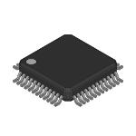
AD9218BSTZ-RL105
Active2-CHANNEL DUAL ADC PIPELINED 105MSPS 10-BIT PARALLEL 48-PIN LQFP T/R
Deep-Dive with AI
Search across all available documentation for this part.

AD9218BSTZ-RL105
Active2-CHANNEL DUAL ADC PIPELINED 105MSPS 10-BIT PARALLEL 48-PIN LQFP T/R
Deep-Dive with AI
Technical Specifications
Parameters and characteristics for this part
| Specification | AD9218BSTZ-RL105 |
|---|---|
| Architecture | Pipelined |
| Configuration | S/H-ADC |
| Data Interface | Parallel |
| Features | Simultaneous Sampling |
| Input Type | Single Ended, Differential |
| Mounting Type | Surface Mount |
| Number of A/D Converters | 2 |
| Number of Bits [custom] | 10 |
| Number of Inputs | 2 |
| Operating Temperature [Max] | 85 °C |
| Operating Temperature [Min] | -40 °C |
| Package / Case | 48-LQFP |
| Ratio - S/H:ADC | 1:1 |
| Reference Type | Internal |
| Sampling Rate (Per Second) | 105 M |
| Supplier Device Package | 48-LQFP (7x7) |
| Voltage - Supply, Analog [Max] | 3.6 V |
| Voltage - Supply, Analog [Min] | 2.7 V |
| Voltage - Supply, Digital [Max] | 3.6 V |
| Voltage - Supply, Digital [Min] | 2.7 V |
Pricing
Prices provided here are for design reference only. For realtime values and availability, please visit the distributors directly
| Distributor | Package | Quantity | $ | |
|---|---|---|---|---|
| Digikey | Tape & Reel (TR) | 2000 | $ 30.16 | |
Description
General part information
AD9218 Series
The AD9218 is a dual 10-bit monolithic sampling analog-to-digital converter with on-chip track-and-hold circuits. The product is low cost, low power, and is small and easy to use. The AD9218 operates at a 105 MSPS conversion rate with outstanding dynamic performance over its full operating range. Each channel can be operated independently.The ADC requires only a single 3.0 V (2.7 V to 3.6 V) power supply and a clock for full operation. No external reference or driver components are required for many applications. The digital outputs are TTL/CMOS compatible and a separate output power supply pin supports interfacing with 3.3 V or 2.5 V logic.The clock input is TTL/CMOS compatible and the 10-bit digital outputs can be operated from 3.0 V (2.5 V to 3.6 V) supplies. User-selectable options offer a combination of power-down modes, digital data formats, and digital data timing schemes. In power-down mode, the digital outputs are driven to a high impedance state.Product HighlightsLow Power. Only 275 mW power dissipation per channel at 105 MSPS. Other speed grades proportionally scaled down while maintaining high ac performance.Pin Compatibility Upgrade. Allows easy migration from 8-bit to 10-bit devices. Pin compatible with the 8-bit AD9288 dual ADC.Easy to Use. On-chip reference and user controls provide flexibility in system design.High Performance. Maintains 54 dB SNR at 105 MSPS with a Nyquist input.Channel Crosstalk. Very low at –75 dBc. 6. Fabricated on an Advanced CMOS Process. Available in a 48-lead low profile quad flat package (7 mm × 7 mm LQFP) specified over the industrial temperature range (−40°C to +85°C).ApplicationsBattery-powered instrumentsHand-held scopemetersLow cost digital oscilloscopesI and Q communicationsUltrasound equipment
Documents
Technical documentation and resources


