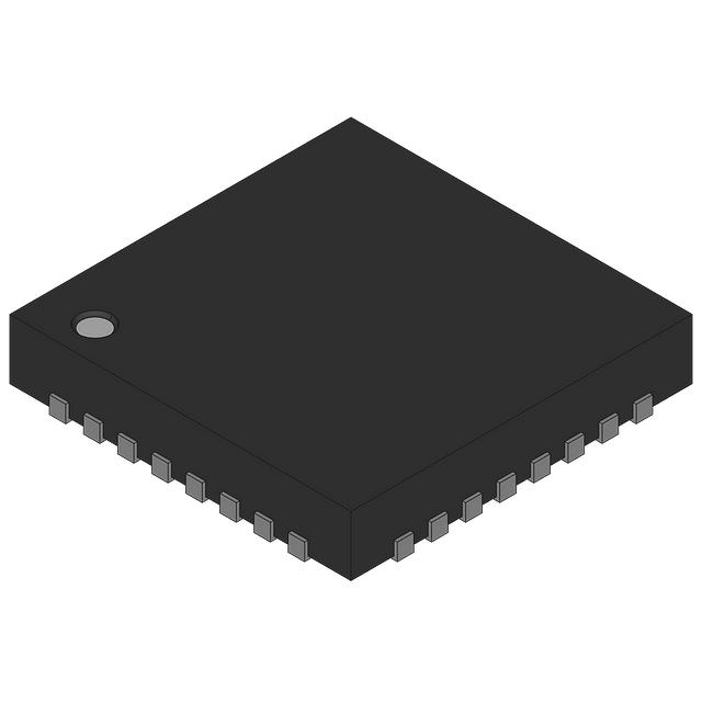
AD8372ACPZ-WP
Active41 DB RANGE, 1 DB STEP SIZE, PROGRAMMABLE DUAL VGA
Deep-Dive with AI
Search across all available documentation for this part.

AD8372ACPZ-WP
Active41 DB RANGE, 1 DB STEP SIZE, PROGRAMMABLE DUAL VGA
Technical Specifications
Parameters and characteristics for this part
| Specification | AD8372ACPZ-WP |
|---|---|
| Applications | CATV |
| Mounting Type | Surface Mount |
| Package / Case | 32-WFQFN Exposed Pad, CSP |
| Supplier Device Package | 32-LFCSP-WQ (5x5) |
| Type | Variable Gain Amplifier |
Pricing
Prices provided here are for design reference only. For realtime values and availability, please visit the distributors directly
| Distributor | Package | Quantity | $ | |
|---|---|---|---|---|
| Digikey | Bulk | 32 | $ 9.50 | |
| 34 | $ 8.99 | |||
Description
General part information
AD8372 Series
The AD8372 is a dual, digitally controlled, variable gain amplifier (VGA) that provides precise gain control, high IP3, and low noise figure. The excellent distortion performance and moderate signal bandwidth make the AD8372 a suitable gain control device for a variety of multichannel receiver applications.For wide input dynamic range applications, the AD8372 provides a broad 41 dB gain range. The gain is programmed through a bidirectional 4-pin serial interface. The serial interface consists of a clock, latch, data input, and data output lines for each channel.The AD8372 provides the ability to set the transconductance of the output stage using a single external resistor. The RXT1 and RXT2 pins provide a band gap derived stable reference voltage of 1.56 V. Typically 2.0 kΩ shunt resistors to ground are used to set the maximum gain to a nominal value of 31 dB. The current setting resistors can be adjusted to manipulate the gain and distortion performance of each channel. This is a flexible feature in applications where it is desirable to trade off distortion performance for lower power consumption.The AD8372 is powered on by applying the appropriate logic level to the ENB1, ENB2 pins. When powered down, the AD8372 consumes less than 2.6 mA and offers excellent input-to-output isolation. The gain setting is preserved when powered down.Fabricated on an Analog Devices, Inc., high frequency BiCMOS process, the AD8372 provides precise gain adjustment capabilities with good distortion performance. The quiescent current of the AD8372 is typically 106 mA per channel. The AD8372 amplifier comes in a compact, thermally enhanced 5 mm × 5 mm 32-lead LFCSP package and operates over the temperature range of −40°C to +85°C.ApplicationsDifferential ADC driversCMTS upstream direct sampling receiversCATV modem signal scalingGeneric RF/IF gain stagesSingle-ended-to-differential conversion
Documents
Technical documentation and resources


