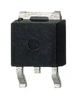
STD60NF55LAT4
ActiveN-CHANNEL 55 V, 12 MOHM, 60 A STRIPFET II POWER MOSFET IN A DPAK PACKAGE

STD60NF55LAT4
ActiveN-CHANNEL 55 V, 12 MOHM, 60 A STRIPFET II POWER MOSFET IN A DPAK PACKAGE
Technical Specifications
Parameters and characteristics for this part
| Specification | STD60NF55LAT4 |
|---|---|
| Current - Continuous Drain (Id) @ 25°C | 60 A |
| Drain to Source Voltage (Vdss) | 55 V |
| Drive Voltage (Max Rds On, Min Rds On) | 10 V, 5 V |
| FET Type | N-Channel |
| Gate Charge (Qg) (Max) @ Vgs | 40 nC |
| Grade | Automotive |
| Input Capacitance (Ciss) (Max) @ Vds | 1950 pF |
| Mounting Type | Surface Mount |
| Operating Temperature [Max] | 175 °C |
| Operating Temperature [Min] | -55 °C |
| Package / Case | TO-252-3, SC-63, DPAK (2 Leads + Tab) |
| Power Dissipation (Max) | 110 W |
| Qualification | AEC-Q101 |
| Rds On (Max) @ Id, Vgs | 15 mOhm |
| Supplier Device Package | TO-252 (DPAK) |
| Technology | MOSFET (Metal Oxide) |
| Vgs (Max) | 15 V |
| Vgs(th) (Max) @ Id | 2 V |
Pricing
Prices provided here are for design reference only. For realtime values and availability, please visit the distributors directly
| Distributor | Package | Quantity | $ | |
|---|---|---|---|---|
| Arrow | N/A | 1 | $ 1.84 | |
| 10 | $ 1.43 | |||
| 50 | $ 1.30 | |||
| 100 | $ 1.00 | |||
| 200 | $ 0.93 | |||
| Digikey | Cut Tape (CT) | 1 | $ 1.67 | |
| 10 | $ 1.39 | |||
| 100 | $ 1.11 | |||
| 500 | $ 0.94 | |||
| 1000 | $ 0.79 | |||
| Digi-Reel® | 1 | $ 1.67 | ||
| 10 | $ 1.39 | |||
| 100 | $ 1.11 | |||
| 500 | $ 0.94 | |||
| 1000 | $ 0.79 | |||
| N/A | 2548 | $ 2.07 | ||
| Tape & Reel (TR) | 2500 | $ 0.75 | ||
| 5000 | $ 0.73 | |||
| 12500 | $ 0.70 | |||
| Newark | Each (Supplied on Cut Tape) | 1 | $ 2.09 | |
| 10 | $ 1.81 | |||
| 25 | $ 1.67 | |||
| 50 | $ 1.54 | |||
| 100 | $ 1.40 | |||
| 250 | $ 1.32 | |||
| 500 | $ 1.25 | |||
| 1000 | $ 1.18 | |||
Description
General part information
STD60 Series
This Power MOSFET series has been developed using STMicroelectronics' unique STripFET™ process, which is specifically designed to minimize input capacitance and gate charge. This renders the device suitable for use as primary switch in advanced high-efficiency isolated DC-DC converters for telecom and computer applications, and applications with low gate charge driving requirements.
Documents
Technical documentation and resources


