Deep-Dive with AI
Search across all available documentation for this part.

Deep-Dive with AI
Technical Specifications
Parameters and characteristics for this part
| Specification | AD8330ARQ |
|---|---|
| -3db Bandwidth | 150 MHz |
| Current - Input Bias | 100 nA |
| Mounting Type | Surface Mount |
| Number of Circuits | 1 |
| Operating Temperature [Max] | 85 °C |
| Operating Temperature [Min] | -40 °C |
| Output Type | Differential, Rail-to-Rail |
| Package / Case | 0.154 in |
| Package / Case | 16-SSOP |
| Package / Case | 3.9 mm |
| Slew Rate | 1500 V/µs |
| Supplier Device Package | 16-QSOP |
| Voltage - Supply Span (Max) [Max] | 6 V |
| Voltage - Supply Span (Min) [Min] | 2.7 V |
Pricing
Prices provided here are for design reference only. For realtime values and availability, please visit the distributors directly
| Distributor | Package | Quantity | $ | |
|---|---|---|---|---|
| Digikey | Tube | 39 | $ 7.77 | |
Description
General part information
AD8330 Series
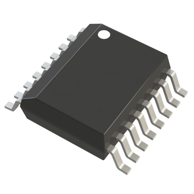
The AD8330 is a wideband variable gain amplifier for applications requiring a fully differential signal path, low noise, well-defined gain, and moderately low distortion, from dc to 150 MHz. The input pins can also be driven from a single-ended source. The peak differential input is ±2 V, allowing sine wave operation at 1 V rms with generous headroom. The output pins can drive single-sided loads essentially rail-to-rail. The differential output resistance is 150 Ω. The output swing is a linear function of the voltage applied to the VMAG pin that internally defaults to 0.5 V, providing a peak output of ±2 V. This can be raised to 10 V p-p, limited by the supply voltage.The basic gain function is linear-in-dB, controlled by the voltage applied to Pin VDBS. The gain ranges from 0 dB to 50 dB for control voltages between 0 V and 1.5 V—a slope of 30 mV/dB. The gain linearity is typically within ±0.1 dB. By changing the logic level on Pin MODE, the gain decreases over the same range, with an opposite slope. A second gain control port is provided at the VMAG pin and allows the user to vary the numeric gain from a factor of 0.03 to 10. All the parameters of the AD8330 have low sensitivities to temperature and supply voltages. Using VMAG, the basic 0 dB to 50 dB range can be repositioned to any value from 20 dB higher (that is, 20 dB to 70 dB) to at least 30 dB lower (that is, –30 dB to +20 dB) to suit the application, thereby providing an unprecedented gain range of over 100 dB. A unique aspect of the AD8330 is that its bandwidth and pulse response are essentially constant for all gains, over both the basic 50 dB linear-in-dB range, but also when using the linearin-magnitude function. The exceptional stability of the HF response over the gain range is of particular value in those VGA applications where it is essential to maintain accurate gain lawconformance at high frequencies.An external capacitor at Pin OFST sets the high-pass corner of an offset reduction loop, whose frequency can be as low as 5 Hz. When this pin is grounded, the signal path becomes dc-coupled. When used to drive an ADC, an external common-mode control voltage at Pin CNTR can be driven to within 0.5 V of either ground or VS to accommodate a wide variety of requirements. By default, the two outputs are positioned at the midpoint of the supply, VS/2. Other features, such as two levels of power-down (fully off and a hibernate mode), further extend the practical value of this exceptionally versatile VGA.The AD8330 is available in 16-lead LFCSP and 16-lead QSOP packages and is specified for operation from −40°C to +85°C.ApplicationsPre-ADC signal conditioning75 Ω cable driving adjustAGC amplifiers
Documents
Technical documentation and resources


