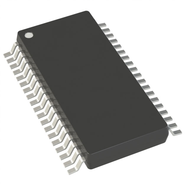
AD5346BRUZ-REEL7
Active2.5 V TO 5.5 V, PARALLEL INTERFACE OCTAL VOLTAGE OUTPUT 8-BIT D/A CONVERTER
Deep-Dive with AI
Search across all available documentation for this part.

AD5346BRUZ-REEL7
Active2.5 V TO 5.5 V, PARALLEL INTERFACE OCTAL VOLTAGE OUTPUT 8-BIT D/A CONVERTER
Deep-Dive with AI
Technical Specifications
Parameters and characteristics for this part
| Specification | AD5346BRUZ-REEL7 |
|---|---|
| Architecture | String DAC |
| Data Interface | Parallel |
| Differential Output | False |
| INL/DNL (LSB) | 0.02 LSB, 0.15 LSB |
| Mounting Type | Surface Mount |
| Number of Bits | 8 |
| Number of D/A Converters | 8 |
| Operating Temperature [Max] | 105 ░C |
| Operating Temperature [Min] | -40 °C |
| Output Type | Voltage - Buffered |
| Package / Case | 38-TFSOP |
| Package / Case [custom] | 4.4 mm |
| Package / Case [custom] | 0.173 in |
| Reference Type | External |
| Settling Time | 8 µs |
| Supplier Device Package | 38-TSSOP |
| Voltage - Supply, Analog [Max] | 5.5 V |
| Voltage - Supply, Analog [Min] | 2.5 V |
| Voltage - Supply, Digital [Max] | 5.5 V |
| Voltage - Supply, Digital [Min] | 2.5 V |
Pricing
Prices provided here are for design reference only. For realtime values and availability, please visit the distributors directly
| Distributor | Package | Quantity | $ | |
|---|---|---|---|---|
| Digikey | Cut Tape (CT) | 1 | $ 13.88 | |
| 10 | $ 9.85 | |||
| 25 | $ 8.82 | |||
| 100 | $ 7.66 | |||
| 250 | $ 7.10 | |||
| 500 | $ 6.76 | |||
| Digi-Reel® | 1 | $ 13.88 | ||
| 10 | $ 9.85 | |||
| 25 | $ 8.82 | |||
| 100 | $ 7.66 | |||
| 250 | $ 7.10 | |||
| 500 | $ 6.76 | |||
| Tape & Reel (TR) | 1000 | $ 6.58 | ||
Description
General part information
AD5346 Series
The AD5346 /AD5347/AD5348are octal 8-, 10-, and 12- bit DACs, operating from a 2.5 V to 5.5 V supply. These devices incorporate an on-chip output buffer that can drive the output to both supply rails, and also allows a choice of buffered or unbuffered reference input.The AD5346 / AD5347 / AD5348 have a parallel interface.CSselects the device and data is loaded into the input registers on the rising edge ofWR. A readback feature allows the internal DAC registers to be read back through the digital port.The GAIN pin on these devices allows the output range to be set at 0 V to VREFor 0 V to 2 x VREF.Input data to the DACs is double-buffered, allowing simultaneous update of multiple DACs in a system using theLDACpin.An asynchronousCLRinput is also provided, which resets the contents of the Input Register and the DAC Register to all zeros. These devices also incorporate a power-on-reset circuit that ensures that the DAC output powers on to 0 V and remains there until valid data is written to the device. All three parts are pin-compatible, which allows the user to select the amount of resolution appropriate for their application without redesigning their circuit board.APPLICATIONSPortable battery-powered instrumentsDigital gain and offset adjustmentProgrammable voltage and current sourcesOptical networkingAutomatic test equipmentMobile communicationsProgrammable attenuatorsIndustrial process control
Documents
Technical documentation and resources


