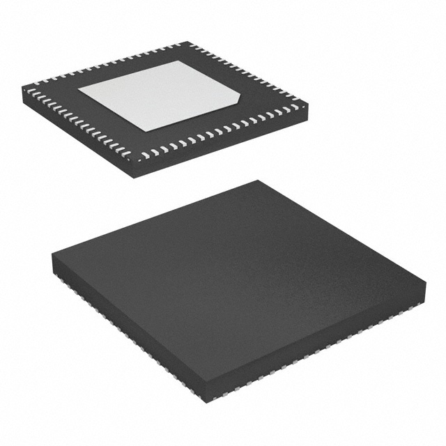
AD9639BCPZ-170
ActiveQUAD 12-BIT, 170/210 MSPS, SERIAL OUTPUT 1.8 V A/D CONVERTER
Deep-Dive with AI
Search across all available documentation for this part.

AD9639BCPZ-170
ActiveQUAD 12-BIT, 170/210 MSPS, SERIAL OUTPUT 1.8 V A/D CONVERTER
Deep-Dive with AI
Technical Specifications
Parameters and characteristics for this part
| Specification | AD9639BCPZ-170 |
|---|---|
| Architecture | Pipelined |
| Configuration | S/H-ADC |
| Data Interface | JESD204 |
| Features | Simultaneous Sampling, Temperature Sensor |
| Input Type | Single Ended, Differential |
| Mounting Type | Surface Mount |
| Number of A/D Converters | 4 |
| Number of Bits | 12 bits |
| Number of Inputs | 4 |
| Operating Temperature [Max] | 85 °C |
| Operating Temperature [Min] | -40 °C |
| Package / Case | 72-VFQFN Exposed Pad, CSP |
| Ratio - S/H:ADC | 1:1 |
| Reference Type | Internal |
| Sampling Rate (Per Second) | 170 M |
| Supplier Device Package | 72-LFCSP-VQ (10x10) |
| Voltage - Supply, Analog [Max] | 1.9 V |
| Voltage - Supply, Analog [Min] | 1.7 V |
| Voltage - Supply, Digital [Max] | 1.9 V |
| Voltage - Supply, Digital [Min] | 1.7 V |
Pricing
Prices provided here are for design reference only. For realtime values and availability, please visit the distributors directly
| Distributor | Package | Quantity | $ | |
|---|---|---|---|---|
| Digikey | Tray | 3 | $ 195.29 | |
| 12 | $ 180.18 | |||
Description
General part information
AD9639 Series
The AD9639 is a quad, 12-bit, 210 MSPS analog-to-digital converter (ADC) with an on-chip temperature sensor and a high speed serial interface. It is designed to support digitizing high frequency, wide dynamic range signals with an input bandwidth up to 780MHz. The output data are serialized per the JESD204 standard. The ADC requires a single 1.8 V power supply and the input clock may be driven differentially with a sine wave, LVPECL, TTL, or LVDS. A clock duty cycle stabilizer allows high performance at full speed with a wide range of clock duty cycles. The on-chip reference removes the need for external decoupling and can be adjusted by means of SPI control.Various power-down and standby modes are supported. The ADC typically consumes 145 mW per channel with the digital link still in operation when standby operation is enabled.Fabricated on an advanced CMOS process, the AD9639 is available in a Pb free/RoHS compliant, 72-lead LFCSP package. It is specified over the industrial temperature range of −40°C to +85°C.PRODUCT HIGHLIGHTSFour ADCs are contained in a small, space-saving package.On chip PLL allows user to provide one ADC sampling clock and the ADC distributes and multiplies up to produce the corresponding data rate clock.Encoded data rate supports up to 4Gbps per channel. Encoding includes 8B/10B to ensure proper DC common mode and embedded clock per JESD204.The AD9639 operates from a single 1.8 V power supply.APPLICATIONSCommunication receiversCable head end equipment/M-CMTSBroadband radiosWireless infrastructure transceiversRadar/mil-aero sub systemsTest equipment
Documents
Technical documentation and resources


