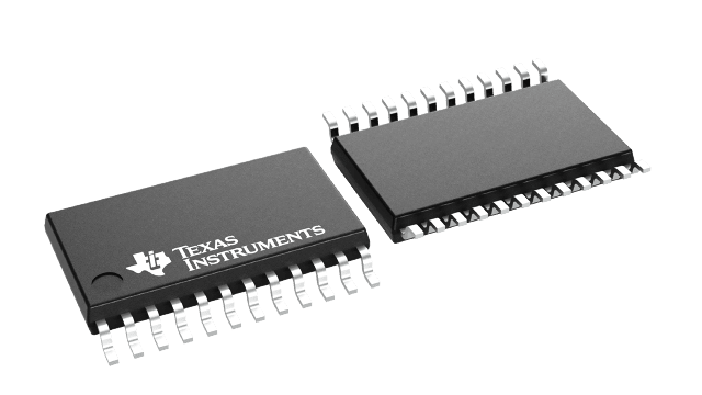
CDCE949QPWRQ1
ActiveAEC-Q100 PROGRAMMABLE 4-PLL VCXO CLOCK SYNTHESIZER WITH 2.5-V OR 3.3-V LVCMOS OUTPUTS
Deep-Dive with AI
Search across all available documentation for this part.

CDCE949QPWRQ1
ActiveAEC-Q100 PROGRAMMABLE 4-PLL VCXO CLOCK SYNTHESIZER WITH 2.5-V OR 3.3-V LVCMOS OUTPUTS
Deep-Dive with AI
Technical Specifications
Parameters and characteristics for this part
| Specification | CDCE949QPWRQ1 |
|---|---|
| Differential - Input:Output | False |
| Divider/Multiplier | Yes/No |
| Frequency - Max [Max] | 230 MHz |
| Grade | Automotive |
| Input | LVCMOS, Crystal |
| Mounting Type | Surface Mount |
| Number of Circuits | 1 |
| Operating Temperature [Max] | 125 °C |
| Operating Temperature [Min] | -40 °C |
| Output | LVCMOS |
| Package / Case | 24-TSSOP |
| Package / Case | 0.173 in, 4.4 mm |
| PLL | Yes with Bypass |
| Qualification | AEC-Q100 |
| Ratio - Input:Output | 1:9 |
| Supplier Device Package | 24-TSSOP |
| Type | Spread Spectrum Clock Driver |
| Voltage - Supply [Max] | 1.9 V |
| Voltage - Supply [Min] | 1.7 V |
CDCE949-Q1 Series
AEC-Q100 programmable 4-PLL VCXO clock synthesizer with 2.5-V or 3.3-V LVCMOS outputs
| Part | Supplier Device Package | Operating Temperature [Max] | Operating Temperature [Min] | Voltage - Supply [Max] | Voltage - Supply [Min] | Number of Circuits | Input | Qualification | PLL | Frequency - Max [Max] | Package / Case | Package / Case | Differential - Input:Output | Type | Divider/Multiplier | Output | Mounting Type | Grade | Ratio - Input:Output | Utilized IC / Part | Supplied Contents | Function |
|---|---|---|---|---|---|---|---|---|---|---|---|---|---|---|---|---|---|---|---|---|---|---|
Texas Instruments | 24-TSSOP | 125 °C | -40 °C | 1.9 V | 1.7 V | 1 | Crystal LVCMOS | AEC-Q100 | Yes with Bypass | 230 MHz | 24-TSSOP | 0.173 in 4.4 mm | Spread Spectrum Clock Driver | Yes/No | LVCMOS | Surface Mount | Automotive | 1:9 | ||||
Texas Instruments | 24-TSSOP | 85 °C | -40 °C | 1.9 V | 1.7 V | 1 | Crystal LVCMOS | Yes with Bypass | 230 MHz | 24-TSSOP | 0.173 in 4.4 mm | PLL Clock Generator | Yes/No | LVCMOS | Surface Mount | 1:9 | ||||||
Texas Instruments | Timing | CDCE949PERF | Board(s) | Clock Generator |
Pricing
Prices provided here are for design reference only. For realtime values and availability, please visit the distributors directly
| Distributor | Package | Quantity | $ | |
|---|---|---|---|---|
| Digikey | Cut Tape (CT) | 1 | $ 6.06 | |
| Digi-Reel® | 1 | $ 6.06 | ||
| Tape & Reel (TR) | 2000 | $ 3.31 | ||
| Texas Instruments | LARGE T&R | 1 | $ 4.64 | |
| 100 | $ 3.79 | |||
| 250 | $ 2.98 | |||
| 1000 | $ 2.52 | |||
Description
General part information
CDCE949-Q1 Series
The CDCE949 and CDCEL949 are modular PLL-based low cost, high-performance, programmable clock synthesizers, multipliers and dividers. These devices generate up to nine output clocks from a single input frequency. Each output can be programmed in-system for any clock frequency up to 230MHz, using up to four independent configurable PLLs.
The CDCEx949 has separate output supply pins (VDDOUT): 1.8V for the CDCEL949 and 2.5V to 3.3V for the CDCE949.
The input accepts an external crystal or LVCMOS clock signal. If an external crystal is used, an on-chip load capacitor is adequate for most applications. The value of the load capacitor is programmable from 0pF to 20pF. Additionally, an on-chip VCXO is selectable, allowing synchronization of the output frequency to an external control signal, that is, a PWM signal.
Documents
Technical documentation and resources


