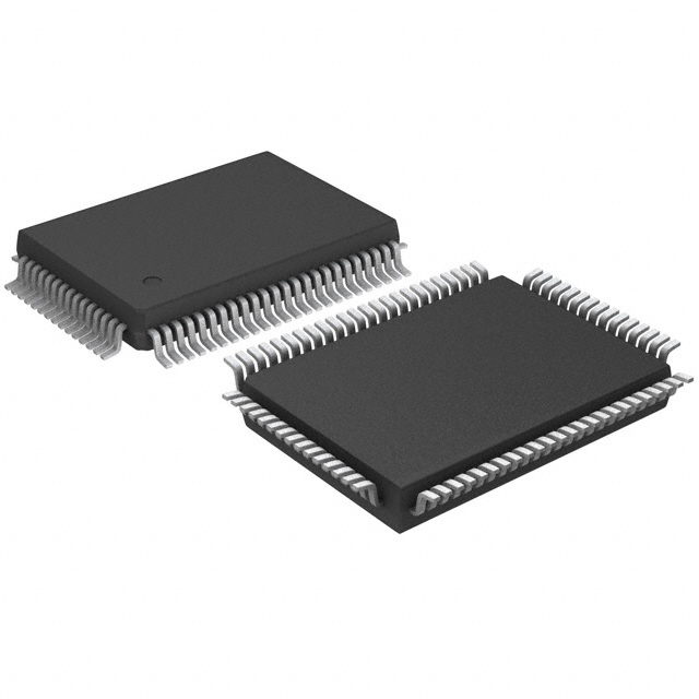
HV507PG-G
Active64-CHANNEL, PUSH PULL, 325V 80 PQFP 20X14X3.4MM TRAY ROHS COMPLIANT: YES
Deep-Dive with AI
Search across all available documentation for this part.

HV507PG-G
Active64-CHANNEL, PUSH PULL, 325V 80 PQFP 20X14X3.4MM TRAY ROHS COMPLIANT: YES
Deep-Dive with AI
Technical Specifications
Parameters and characteristics for this part
| Specification | HV507PG-G |
|---|---|
| Function | Serial to Parallel |
| Logic Type | Shift Register |
| Mounting Type | Surface Mount |
| Number of Bits per Element | 64 |
| Number of Elements | 1 |
| Operating Temperature [Max] | 70 °C |
| Operating Temperature [Min] | 0 °C |
| Output Type | Push-Pull |
| Package / Case | 80-BQFP |
| Supplier Device Package | 80-PQFP (14x20) |
| Voltage - Supply [Max] | 5.5 V |
| Voltage - Supply [Min] | 4.5 V |
Pricing
Prices provided here are for design reference only. For realtime values and availability, please visit the distributors directly
| Distributor | Package | Quantity | $ | |
|---|---|---|---|---|
| Digikey | Tray | 1 | $ 19.99 | |
| 25 | $ 16.65 | |||
| 100 | $ 16.09 | |||
| Microchip Direct | TRAY | 1 | $ 19.99 | |
| 25 | $ 16.65 | |||
| 100 | $ 15.14 | |||
| 1000 | $ 14.60 | |||
| 5000 | $ 14.47 | |||
| Newark | Each | 25 | $ 16.96 | |
| 100 | $ 15.60 | |||
Description
General part information
HV507 Series
The HV507 is a low voltage serial to high voltage parallel converter with 64 push-pull outputs. This device has been designed for use as a printer driver for electrostatic applications. It can also be used in any application requiring multiple output, high voltage, low current sourcing and sinking capabilities.
The device consists of a 64-bit shift register, 64 latches, and control logic to perform the polarity select and blanking of the outputs. A DIR pin controls the direction of data shift through the device. With DIR grounded, DIOA is Data-In and DIOB is Data-Out; data is shifted from HVOUT64 to HVOUT1. When DIR is at logic high, DIOB is Data-In and DIOA is Data-Out: data is then shifted from HVOUT1 to HVOUT64. Data is shifted through the shift register on the low to high transition of the clock. Data output buffers are provided for cascading devices. Operation of the shift register is not affected by the LE (latch enable), BL (blanking), or the POL(polarity) inputs. Transfer of data from the shift register to the latch occurs when the LE is high. The data in the latch is stored during LE transition from high to low.
Documents
Technical documentation and resources


