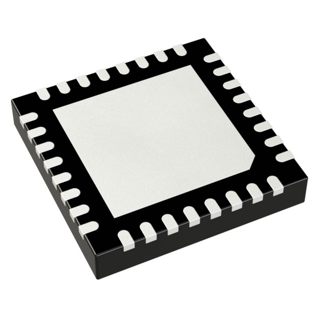
HMC987LP5ETR
Obsolete3.3V LOW NOISE 1:9 FANOUT BUFFER, DC - 8 GHZ
Deep-Dive with AI
Search across all available documentation for this part.

HMC987LP5ETR
Obsolete3.3V LOW NOISE 1:9 FANOUT BUFFER, DC - 8 GHZ
Deep-Dive with AI
Technical Specifications
Parameters and characteristics for this part
| Specification | HMC987LP5ETR |
|---|---|
| Differential - Input:Output [custom] | True |
| Differential - Input:Output [custom] | True |
| Frequency - Max [Max] | 8 GHz |
| Input | CML, LVPECL, LVDS, CMOS |
| Mounting Type | Surface Mount |
| Number of Circuits | 1 |
| Operating Temperature [Max] | 85 °C |
| Operating Temperature [Min] | -40 °C |
| Output | LVPECL, CML |
| Package / Case | 32-VFQFN Exposed Pad |
| Ratio - Input:Output | 1:9 |
| Supplier Device Package | 32-QFN (5x5) |
| Type | Fanout Buffer (Distribution) |
| Voltage - Supply [Max] | 3.6 V |
| Voltage - Supply [Min] | 3 V |
Pricing
Prices provided here are for design reference only. For realtime values and availability, please visit the distributors directly
| Distributor | Package | Quantity | $ | |
|---|---|---|---|---|
Description
General part information
HMC987 Series
The HMC987LP5E 1-to-9 fanout buffer is designed for low noise clock distribution. It is intended to generate relatively square wave outputs with rise/fall times < 100 ps. The low skew and jitter outputs of the HMC987LP5E, combined with its fast rise/fall times, leads to controllable low-noise switching of downstream circuits such as mixers, ADCs/DACs or SERDES devices. The noise floor is particularly important in these applications, when the clocknetwork bandwidth is wide enough to allow squarewave switching. Driven at 2 GHz, outputs of the HMC987LP5E have a noise floor of –166 dBc/Hz, corresponding to a jitter density of 0.6 asec/rtHz - or 50 fs over an 8 GHz bandwidth.The input stage can be driven single-ended or differentially, in a variety of signal formats (CML, LVDS, LVPECL or CMOS), AC or DC coupled. The input stage also features adjustable input impedance. It has 8 LVPECL outputs, and 1 CML output with adjustable swing/power-level in 3 dB steps.Individual output stages may be enabled or disabled for power-savings when not required using either hardware control pins, or under control of a serial-port interface.APPLICATIONSSONET, Fibre Channel, GigE Clock DistributionADC/DAC Clock DistributionLow Skew and Jitter Clock or Data FanoutWireless/Wired CommunicationsLevel TranslationHigh Performance InstrumentationMedical ImagingSingle-Ended to Differential Conversion
Documents
Technical documentation and resources


