Deep-Dive with AI
Search across all available documentation for this part.

Deep-Dive with AI
Technical Specifications
Parameters and characteristics for this part
| Specification | AD7466BRM-REEL |
|---|---|
| Data Interface | DSP, SPI |
| Mounting Type | Surface Mount |
| Number of A/D Converters | 1 |
| Number of Bits | 12 bits |
| Operating Temperature [Max] | 85 °C |
| Operating Temperature [Min] | -40 °C |
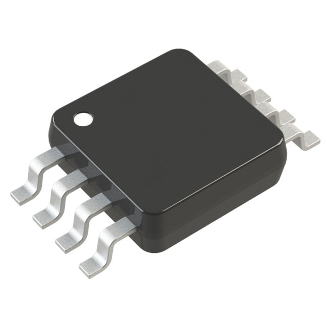
| Package / Case | 8-MSOP, 8-TSSOP |
| Package / Case | 3 mm |
| Package / Case [custom] | 0.118 in |
| Sampling Rate (Per Second) | 200k |
| Supplier Device Package | 8-MSOP |
Pricing
Prices provided here are for design reference only. For realtime values and availability, please visit the distributors directly
| Distributor | Package | Quantity | $ | |
|---|---|---|---|---|
| Digikey | Bulk | 72 | $ 4.20 | |
Description
General part information
AD7466 Series
The AD7466 / AD7467 / AD7468 are 12-/10-/8-bit, high speed, low power, successive approximation analog-to-digital converters (ADCs), respectively. The parts operate from a single 1.6 V to 3.6 V power supply and feature throughput rates up to 200 kSPS with low power dissipation. The parts contain a low noise, wide bandwidth track-and-hold amplifier, which can handle input frequencies in excess of 3 MHz.The conversion process and data acquisition are controlled usingCSand the serial clock, allowing the devices to interface with microprocessors or DSPs. The input signal is sampled on the falling edge ofCS, and the conversion is also initiated at this point. There are no pipeline delays associated with the part.The reference for the part is taken internally from VDD. This allows the widest dynamic input range to the ADC. Thus, the analog input range for the part is 0 V to VDD. The conversion rate is determined by the SCLK.PRODUCT HIGHLIGHTSSpecified for supply voltages of 1.6 V to 3.6 V12-, 10-, and 8-bit ADCs in SOT-23 and MSOP packagesHigh throughput rate with low power consumption. Power consumption in normal mode of operation at 100 kSPS and 3 V is 0.9 mW maximumFlexible power/serial clock speed management. The conversion rate is determined by the serial clock, allowing the conversion time to be reduced through increases in the serial clock speed. Automatic power-down after conversion allows the average power consumption to be reduced when in power-down. Current consumption is 0.1 μA maximum and 8 nA typically when in power-downReference derived from the power supplyNo pipeline delayThe part features a standard successive approximation ADC with accurate control of conversions via aCSinputAPPLICATIONSBattery-powered systemsMedical instrumentsRemote data acquisitionIsolated data acquisition
Documents
Technical documentation and resources


