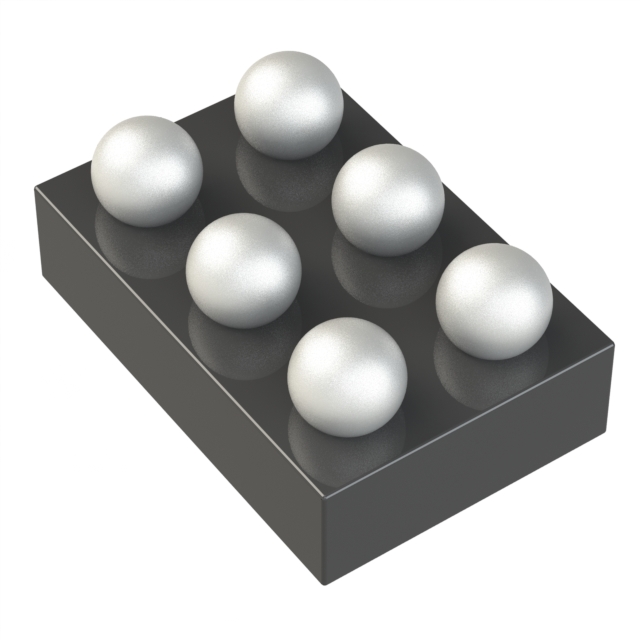
ADL5507ACBZ-R7
Active10 MHZ TO 12 GHZ, 55 DB LOGARITHMIC RF POWER DETECTOR
Deep-Dive with AI
Search across all available documentation for this part.

ADL5507ACBZ-R7
Active10 MHZ TO 12 GHZ, 55 DB LOGARITHMIC RF POWER DETECTOR
Deep-Dive with AI
Technical Specifications
Parameters and characteristics for this part
| Specification | ADL5507ACBZ-R7 |
|---|---|
| Accuracy | 1 dB |
| Current - Supply | 12.5 mA |
| Frequency [Max] | 12 GHz |
| Frequency [Min] | 10 MHz |
| Input Range [Max] | -1 dBm |
| Input Range [Min] | -56 dBm |
| Mounting Type | Surface Mount |
| Package / Case | WLCSP, 6-XFBGA |
| RF Type | General Purpose |
| Supplier Device Package | 6-WLCSP |
| Supplier Device Package [x] | 0.76 |
| Supplier Device Package [y] | 1.36 |
| Voltage - Supply [Max] | 3.45 V |
| Voltage - Supply [Min] | 2.7 V |
Pricing
Prices provided here are for design reference only. For realtime values and availability, please visit the distributors directly
| Distributor | Package | Quantity | $ | |
|---|---|---|---|---|
| Digikey | Tape & Reel (TR) | 3000 | $ 3.92 | |
Description
General part information
ADL5507 Series
The ADL5507 is a complete, low-power, wide-band logarithmic RF power detector for the measurement of RF signals in the 10 MHz to 12 GHz frequency range. The device is optimized for accurate RF signal level measurements over a 55 dB dynamic range, from −56 dBm to −1 dBm at 3.6 GHz, when terminated with 50 Ω. It provides a wider dynamic range and better accuracy than is possible using discrete diode detectors. Its high sensitivity allows measurement of low power levels, thus reducing the amount of power that needs to be coupled to the detector.For convenience, the signal input is internally AC-coupled, using a series 25 pF capacitor. Therefore, the source can be DC grounded. A broadband 50 Ω match is obtained with an external 51 Ω shunt resistor. This high-pass coupling, with a corner at approximately 4 MHz, determines the lowest operating frequency.The DC voltage at the ADL5507 output interface responds linearin- dB to the RF signal level applied at its input. It is accurately temperature compensated to provide typically better than ±1 dB measurement accuracy over the full case operating temperature range from −40°C to +105°C. The output interface has sufficient capability to drive a wide range of analog‐to‐digital converters (ADCs) and other circuitry.The CFLT interface enables additional ripple and noise filtering of the output signal, without reducing the drive capability of the VLOG interface. This is achieved by connecting a capacitor between the CFLT and VLOG interfaces.The tri-state ENBL interface switches the device between active positive output slope mode, active negative output slope mode, and a low-power shutdown mode. In positive output slope mode, the ADL5507 output increases approximately from 0.1 V to 1.2 V as the input signal level increases from 0.35 mV rms (−56 dBm) to 200 mV rms (−1 dBm). In negative output slope mode, the output decreases approximately from 1 V to 0 V as the input signal level decreases from 200 mV rms (−1 dBm) to 0.35 mV rms (−56 dBm). The output interface becomes high impedance in shutdown to avoid discharge of external filter capacitors.The ADL5507 is available in a 6-ball WLCSP package and consumes 12.5 mA from a 3.3 V supply. In shutdown mode, the typical disable supply current is <100 μA.APPLICATIONSRSSI and TSSI for wired and wireless terminal devicesRF transmitter or receiver power measurementWide-band Automatic Gain Control
Documents
Technical documentation and resources


